
|
 news releases news releases |
|
|
|
 PDF Download(PDF Type, 37Kbyte) PDF Download(PDF Type, 37Kbyte) |
|
| January 15, 2004 |
|
| Hitachi releases 144-Mbit Cache DRAM "HDL5KM Series" with world-leading 8ns random access time and 4GB/s data bandwidth |
|
|
|
 |
|
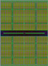
| 144-Mbit cache DRAM "HDL5KM series" |
|
Tokyo, January 15, 2004 - Hitachi Ltd.,(TSE:6501,NYSE:HIT) today announced the high-performance 144-Mbit cache (*1) DRAM "HDL5KM series" with world-leading 8ns (*2) random access time and 4GB/s (*3) data bandwidth. Sample shipments will begin on June 1, 2004.
| (*1) |
Cache (memory) : A high-speed memory located between the microprocessor and main memory. It is used to improve server performance by storing frequently-used data and reducing access to the slow-speed main memory. |
| (*2) |
ns (nanosecond) : One-billionth of a second |
| (*3) |
GB/s (gigabyte / second) : One billion bytes per second |
To realize high-performance operation of computers and network equipment, high-speed SRAMs have been used in their memory systems. For further improvement of such systems, large capacity memories such as DRAMs operating at high-speed equivalent to that of SRAMs are much sought after.
The new series was developed by Hitachi's Device Development Center, using the leading-edge high-speed embedded DRAM process, realizes both large memory capacity of 144Mbit and SRAM-level high-speed performance. Adopting the new series to cache memory of high-performance servers, buffer memory (*4) or table memory (*5) of network equipment such as routers and switches, brings further improvement of their performance.
| (*4) |
Buffer memory : A temporal storage of packet data used in network equipment |
| (*5) |
Table memory : A storage of packet addresses for which destination addresses are searched in network systems |
| - Major features of the "HDL5KM Series" |
1. Large capacity cache DRAM of 144Mbit
The new series is realized by using leading-edge high-speed embedded DRAM process, packaged in a standard BGA package which is compatible with that of SRAMs
The new series enables memory systems with capacity of 4 to 8 times as large as SRAM-based systems, which means that the price per bit can be lower than one forth of SRAMs, leading to great amount of cost reduction of the systems.
2. High-speed operation of 8ns random access time and 4GB/s data bandwidth
The random access time and random cycle time of the new series are both 8ns and read operations or write operations can be performed at 4GB/s maximum bandwidth, such features being equivalent to those of SRAMs. Late write function (*6) adopted in the new series avoids conflicts between read data and write data at the input/output buses, which leads to highly efficient bus utilization.
These characteristics enable fast processing of large data and contribute to performance improvement of computers and network equipment.
| (*6) |
Late write function : A function to set the timing of write data input to be the same as the timing of read data output |
3. Ready to satisfy wide user needs
In addition to variation of the number of data bits simultaneously written or read, x36 and x18, the lineup of the number of banks (single or 16) (*7) is provided. Users can select the optimal product with such features which satisfies their system needs, such as servers, network equipment and image processing systems.
| (*7) |
Bank : A unit of memory blocks which can perform read operations or write operations independently from the other blocks |
| Product Name |
Sample price |
Sample availability |
| HDL5KM series |
25,000 JPY (*8) |
June 1, 2004 |
|
| (*8)Individual estimate will be provided, based on quantities and conditions |
| - Indication about other companies' trademarks |
| The described company names and product names are trademarks or registered trademarks of the respective companies. |
| - About the Device Development Center |
| The Device Development Center is developing and producing LSIs for such information and communications equipment as storage systems, networking devices and cutting-edge industrial appliances for both the Hitachi group companies and non-group customers. It also performs development of semiconductor-related technologies by commission and foundry business. |
| - References |
Person in charge: Kojima
Planning Office, Device Development Center,
Information and Telecommunication Systems, Hitachi, Ltd.
6-16-3, Shinmachi, Ome-shi, Tokyo 198-8512
+81-428-33-2011 (direct dialing)
E-Mail: www-info@ddc.hitachi.co.jp |
|
|
|
| Information contained in this news release is current as of the date of the press announcement, but may be subject to change without prior notice. |
|
|
 |
PDF files are in Adobe's Portable Document Format. To view them you need Adobe® Reader® 6.0 by Adobe Systems Incorporated. If you are using Adobe Acrobat® 5.x software, you will need to download Asian font packs. |
|
|
|
|
|