|
 News releases News releases |
|
|
|
 PDF Download(PDF Type, 114Kbyte) PDF Download(PDF Type, 114Kbyte) |
|
| February 6, 2006 |
|
| World's smallest and thinnest 0.15 x 0.15 mm, 7.5µm thick RFID IC chip |
|
| - Enhanced productivity enabled by 1/4 surface area, 1/8th thickness - |
|
|
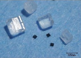
Tokyo, 6th February 2006 --- Hitachi, Ltd. (NYSE:HIT / TSE:6501) today announced it has developed and verified operation of a 0.15 x 0.15 millimeter (mm), 7.5 micrometer (µm)*1 thick contactless IC chip, the smallest and thinnest in the world, to date. The chip is a smaller version of the 0.4 x 0.4 mm "µ-Chip"*2 currently being marketed by Hitachi, maintaining the same level of functionality. The distance between each circuit element was reduced by using SOI technology,*3 which has an insulating layer in the substrate, instead of the Si (silicon) only substrate currently being used. Compared to the 0.3 x 0.3 mm, 60µm thick IC chip*4(henceforth 0.3mm IC chip) announced by Hitachi in February 2003, surface area is reduced to a quarter of the original size. Developments in thin chip fabrication technology have also enabled the chip to be reduced to one-eighth the thickness of the 0.3mm IC chip, at the same time. This significant decrease in size, increases the number of chips which can be fabricated on a single wafer, thus increasing productivity by more than four times. Compared to the current product which was used at the 2005 World Exposition held in Aichi, Japan, productivity is increased by about 10 times. This technology is expected to open the way to new applications for contactless IC chips.
The µ-Chip is one of the world's smallest contactless IC chips which uses an external antenna to receive radio waves (2.45 GHz microwaves), and transforms it to energy to wirelessly transmit a 128 bit (1038) unique ID number. As the data is written during the fabrication process using ROM (Read-Only-Memory), it is impossible to rewrite the data and thus provides a high level of authenticity. The admission ticket system for the 2005 World Exposition, which had approximately 22,050,000 visitors, employed the µ-Chip, has a performance record of no incidence of confirmed forgery and 0.001% incidence of ticket recognition error. By taking advantage of the merits of compactness, high authenticity and contactless communication, and combining it with Internet technology, the µ-Chip may be utilized in a broad range of applications such as security, transportation, amusement, traceability and logistics.
Hitachi has been working on technology such as increasing communication distance and decreasing antenna size, whilst maintaining those merits, to enable a broader range of applications for the µ-Chip. The enhanced compactness and thinness of this new chip has further broadened the range of possible applications, including securities like gift certificates and a large variety of certificates. Further, as with the 0.3mm IC chip, the new chip has a double-surface electrode, and therefore despite its even smaller size, connection with the external antenna can be easily achieved, and high productivity maintained.
 Features of the IC chip developed Features of the IC chip developed |
 (1) World's smallest size achieved through application of SOI technology (1) World's smallest size achieved through application of SOI technology |
| In the past, to prevent malfunction as a result of interference from neighboring devices, a wide device separation region was necessary around high frequency devices. Using SOI process, each device was surrounded by insulator, thus even when the devices were located in close proximity, interference between devices could be prevented and thus higher integration achieved on an even smaller area. |
| |
| (2) Thin chip achieved through application of SOI technology |
| This was achieved by complete removal of the silicon layer on the reverse side of the SOI substrate on which the circuit is fabricated. |
These results will be presented at the IEEE International Solid-State Circuits Conference (ISSCC 2006), being held from 5th - 9th February 2006, in San Francisco, California, U.S.A.
| Notes |
| *1) |
1µm = 1 micrometer; one thousandth of a millimeter (10-3 mm) |
| *2) |
"µ-Chip" and the µ-Chip Logo are either registered trademarks or trademarks of Hitachi, Ltd. in Japan and in other countries. |
| *3) |
Silicon-on-Insulator (SOI): A new fabrication process technology receiving much attention as a method for increasing transistor performance efficiency. In the conventional fabrication process, a transistor is formed directly upon the silicon substrate. In the SOI process, an insulation layer and a monocrystalline silicon layer (referred to as silicon on insulator) is formed upon the base silicon substrate, and the transistor is formed on this SOI substrate. Parasitic capacitance and leakage current are significantly reduced compared to the conventional process, and therefore transistor performance is increased. |
| *4) |
The 0.3 x 0.3 mm, 60 µm thick double-surface electrode IC chip was presented at ISSCC 2003. It is different from the IC chip currently in mass production. |
| About Hitachi, Ltd. |
| Hitachi, Ltd., (NYSE: HIT), headquartered in Tokyo, Japan, is a leading global electronics company with approximately 347,000 employees worldwide. Fiscal 2004 (ended March 31, 2005) consolidated sales totaled 9,027.0 billion yen ($84.4 billion). The company offers a wide range of systems, products and services in market sectors including information systems, electronic devices, power and industrial systems, consumer products, materials and financial services. For more information on Hitachi, please visit the company's website at http://www.hitachi.com |
|
|
|
| Information contained in this news release is current as of the date of the press announcement, but may be subject to change without prior notice. |
|
|
 |
PDF files are in Adobe's Portable Document Format. To view them you need Adobe(R) Reader(R) by Adobe Systems Incorporated. |
|
|
|
|
|