 |
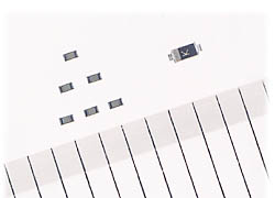
| Diodes Using CSD Package |
| Left:HVZ500(CSD Package) Right:Previous Package(SFP) |
Tokyo, November 26, 2001 — Hitachi, Ltd. (TSE: 6501) today announced
the development of the CSD (Chip Scale Diode: Hitachi package code)
package as the industry's smallest diode package for portable products,
and the release of the HVZ500 and HVZ501 variable capacitance diodes*1
ideal for voltage controlled oscillator (VCO)*2
use in mobile phones, and the HVZ800 PIN diode*3
for RF switch use, as the initial products using this package. Sample
shipments will begin in December 2001 in Japan.
The CSD package features a 0.6  0.3 (mm) level size--generally called 0603 type--that offers a mounting
area approximately 1/5 that of the previous 1406 type. The new package
is also only 0.3 mm (typ.) thick, enabling application products to
be made smaller and thinner.
0.3 (mm) level size--generally called 0603 type--that offers a mounting
area approximately 1/5 that of the previous 1406 type. The new package
is also only 0.3 mm (typ.) thick, enabling application products to
be made smaller and thinner.
[Background]
There is a growing demand for smaller, slimmer models in the field
of portable products such as mobile phones, bringing calls for smaller
and thinner electronic devices for various modules such as VCOs and
antenna switches installed in such products. Hitachi has previously
had a variety of small-package diodes in mass production, and is now
releasing three diode products that achieve ultra-small and thin dimensions
of 0.62 0.32
0.3 (mm) (typ.) through new package development and a revised chip
structure.
[About these Products]
The newly developed CSD employs a structure in which both electrodes,
anode and cathode, are located on the same surface. The CSD can be
directly mounted on a board, and the elimination of leads as required
by previous packages has resulted in the world's smallest size for
a diode of 0.62 0.32
0.3 (mm)(typ.). This represents an approximately 80% reduction in
mounting area and approximately 45% reduction in thickness compared
with the currently smallest 1406 type SFP (Hitachi package code),
enabling end products to be made smaller and slimmer.
The electrodes also have a lead-free specification that makes them
ideal from an environmental viewpoint.
The following three diode products are being released as initial CSD
products.
(1) Variable capacitance diodes for VCO use
HVZ500: 10 V maximum rating, 2.43 (min.)
capacitance ratio
HVZ501: 15 V maximum rating, 2.0 (min.)
capacitance ratio
(2) PIN diode for RF switch use
HVZ800: 0.7 (max.) on-resistance at 2 mA, 1.0 pF (max.) inter-pin capacitance
Ongoing CSD developments will include models such as PIN diodes for
antenna switch use. In addition, future plans call for extension of
the lineup of various diodes to cover a wider application area including
PDAs and notebook PCs.
| Notes: 1. |
|
Variable capacitance diode: Characterized
by variation of capacitance according to the applied reverse voltage.
This property is used for VCO frequency regulation. |
| 2. |
|
VCO: Voltage controlled oscillator.
A unit that performs frequency regulation by means of voltage
variation. |
| 3. |
|
PIN diode: A diode in which an I layer (Intrinsic
layer) is inserted between a P-type semiconductor and N-type semiconductor
to form a PIN junction. Mainly used in digital cellular phone
system antenna switches and multimedia tuner source switching
applications. |
< Typical Applications >
| (1) |
Variable capacitance diodes |
 |
Voltage controlled oscillators (VCOs) for mobile
phones |
|
Voltage controlled crystal oscillators (VCXOs)
for mobile phones |
| (2) |
PIN diode |
|
RF switches |
< Prices in Japan >(For Reference)
| Part Number |
Type |
Package |
Sample Price (Yen) |
| HVZ500 |
Variable capacitance
diode
for VCO use |
CSD |
15 |
| HVZ501 |
15 |
| HVZ800 |
PIN diode for RF switch use |
15 |
< Specifications >
(1) HVZ500 and HVZ501 variable capacitance diodes for VCO use
Part
Number
|
Package
|
Maximum Rated
Reverse Voltage
VR (V) |
Inter-Pin
Capacitance
C (pF) |
Capacitance
Ratio
n |
Series
Resistance
rs () |
HVZ500
|
CSD
|
10
|
C0.5 = 7.20 to 7.70
C2.5 = 2.70 to 3.20 |
2.43(min.)
@C0.5/C2.5 |
0.75(max.)
|
HVZ501
|
CSD
|
15
|
C1 = 15.0 to 17.0
C4 = 7.0 to 8.5 |
2.0(min.)
@C1/C4 |
0.4(max.)
|
(2) HVZ800 PIN diode for RF switch use
Part
Number |
Package |
Maximum Rated
Reverse Voltage
VR (V) |
Forward Voltage
VF (V) |
Inter-Pin Capacitance
C (pF) |
On-Resistance
rf () |
HVZ500
|
CSD
|
30
|
0.85 (max.)
@2 mA |
C1 = 1 (max.) |
0.7 (max.)
@IF = 2 mA
f = 100 MHz |
|