| GLOBAL HOME | UP | SEARCH |
News Releases from Headquarters


PDF DOWNLOAD


Hitachi Announced "superAND Type Flash Memory",
Flash Memory with Built-in Memory Control Function For the First Time In the Industry
- Easy-to-use compact memory for data storage for mobile phones and PDA at reasonable price -
 
128-Mbit superAND type flash memory
Left:HN29A128A(CSP) Center:HN29A128A(TSOP-I) Right:HN29V128A(TSOP-I)

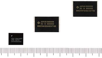
Tokyo, April 2, 2002 — Hitachi, Ltd. (TSE: 6501) today announced "superAND type flash memory" suitable for portable devices such as mobile phones and PDA. This new AND type flash memory has dramatically improved the easy-to-use feature by incorporating a memory control function in the flash memory for the first time in the industry, and also achieved a compact size and a reasonable price. For the initial release, Hitachi is releasing a total of four types, "HN29V128A (3.3V type)" and "HN29A128A (1.8V type) series of 128M bits (16M bytes). Sample shipment will begin from June 2002 in Japan.

Flash memory defective sectors are normally controlled by an external controller or a hardware/software on the equipment installed. This product incorporates a flash memory defective sector control*1 function within the flash memory for the first time in the industry and, achieving 100% full operation of the memory area after shipment. Also with built-in wear leveling function*2 this product facilitates system design using flash memory. By design optimization, increase of chip size was minimized to only a few percent of Hitachi's conventional monolithic flash memory, enabling a compact size and reasonable price.

Hitachi is aiming at introduction of this "superAND type flash memory" as a de facto standard to be used as embedded data storage memory for portable devices.

[Background]

Recently, the sizes of memory units installed in portable equipment such as mobile phones and PDA are expanding with the increase of the amount of information due to multifunctionality and increase of distribution of various contents. However, to use the AND type flash memory that is suitable for data storage as embedded memory, complicated problems must be resolved such as designing a new complicated control system for flash memory for defective sector control or use of the memory with a controller for memory control.

Hitachi developed "superAND type flash memory" that achieved improved operability and compact size by incorporating a memory control function in the AND type flash memory while minimizing the chip size increase to a few percent, based on the technology that was developed through controller development of flash card such as CompactFlashTM*3 and MultiMediaCardTM*4.

[About these products]

For the initial release, the "HN29V128A (3.3 V type)" and "HN29A128A (1.8 V type)" Series of 128 M bits (16 M bytes), which were announced as the first release, use 0.18 m process multi-level cell flash memory process, achieving large capacity and compact size features by application of multi-level cell technology*5. The optimization design achieved the memory control function on-chip installation within a compact size. The main features are as follows.

1. Dramatic improvement of operability

(1) Built-in memory control function for the first time in the flash memory industry
Conventional AND type flash memory contains maximum 2% of defector sectors at shipment. Defective sectors may occur in any conventional flash memory after shipment and these defective sectors need to be controlled by hardware or software on the equipment installation side, or a controller needs to be installed.
The "superAND type flash memory" incorporates a defective sector control function in the flash memory for the first time in the industry. Even if abnormality occurs in some sectors during operation, the flash memory detects defects and automatically replaces defective sectors with reserved sectors.
In this way, a 100% full operation of a memory area is achieved regardless of before or after shipment within the life span, utilizing a design of a system that incorporates flash memory.

(2) Built-in ware leveling function (flash life span stretching )
Since chips become fragile if writing is concentrated on the same section, the function automatically replaces data and addresses with areas that are less used for rewriting when rewriting to some area reach a certain count. The built-in ware leveling function can increase the life span of rewriting of flash memory.
 
(3) Support of a Power On Read function (2K bytes size)
When a system is started by turning on the power, data up to 2K bytes can be read by controlling two control lines (CE pin and RE pin) without inputting any command or address.
   
(4) Support of a deep standby function
A deep standby function is supported for portable electronic equipment that requires extreme power supply control. At deep standby, the current can be reduced to 5 micro A.
   
(5) Lineup of two types of operation voltages and bus width
Operation voltages of 3.3 V (HN29V128A) and 1.8 V (HN29A28A) and bus widths of 8 bits (3.3 V type only) and 16 bits are available, enabling selection of a product suitable for system design.

2. Compact size and reasonable price

  The optimization design of the controller section achieved on-chip installation of a memory control function by a mere few percent of size increase, thereby achieving a compact size. For the memory cells, Hitachi's high cost competitive 0.18 m process multi-level cell AND type flash memory is used, providing large capacity memory at a reasonable price.

Since the NAND type interface is used, the product can be made compatible to the systems that use the existing NAND type flash memory with small software modifications.

The product uses a 48-pin TSOP type 1 as the package. The product of operation voltage 1.8 V and 16 bits is also equipped with a smaller 72- bump CSP (HN29A128A0ABP-80).

[Development support tools]

As the support tools for designing systems using this flash memory, Hitachi will release a VHDL model as the functional description model, an IBIS model as the I/O operation model, and a reference driver model in C language from June 2002.

For further increase of capacity, Hitachi will introduce 256M-bit products and 512M-bit products.

Notes: 1. Defective sector control: Control operation by detecting defects when an abnormality occurs in some sectors in flash memory and replacing defective sectors with reserved sectors.
2. Wear leveling function: Since chips become fragile if writing is concentrated on the same section, the function replaces data and addresses with areas that are less used for rewriting when rewriting to some area reach a certain count.
3. CompactFlashTM : CompactFlash is a trademark of SanDisk Corporation of the United States and is licensed to the CFA (CompactFlash Association). Hitachi, Ltd. is a member of the CFA. http://www.compactflash.org/
4. MultiMediaCardTM : MultiMediaCard is a trademark of Infineon Technologies AG of Germany, and is licensed to the MMCA (MultiMediaCard Association). Hitachi, Ltd. is an MMCA board member. http://www.mmca.org/
5. Multi-level cell technology: This technology is suitable for large capacity flash memory suitable for chip downsizing. While normal memory stores two values '0' and '1', in this technology, memory stores four or more values 00, 01, 10, 11, etc. When four values are stored, one cell achieves the functions for two cells.

< Typical Applications >
Mobile phones
Portable information terminals such as PDA
Portable image equipment such as digital camera

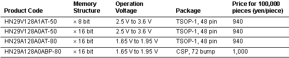
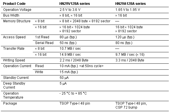
< Prices in Japan >(For Reference)


< Specifications >


Information contained in this news release is current as of the date of the press announcement, but may be subject to change without prior notice.


top of this page
WRITTEN BY Corporate Communications Division
(C) Hitachi,Ltd. 1994,2002. All rights reserved.