 |
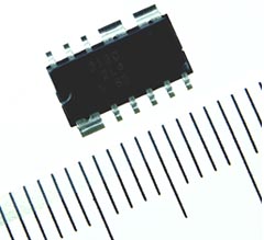
| “HAT2180RP” Composite Power MOSFET |
Tokyo, December 9, 2002— Hitachi, Ltd. (TSE: 6501) today announced the HAT2180RP 30 V Drain-Source breakdown voltage Composite power MOSFET incorporating the equivalent of three elements--a power MOSFET with a built-in Schottky barrier diode, and another power MOSFET--in a single package, for non-isolated DC/DC converters used in products such as notebook PCs. Sample shipments will begin on December 10, 2002 in Japan.
The non-isolated DC/DC converter comprises a high-side switch and low-side switch, with a power MOSFET used for each. In HAT2180RP, the power MOSFET for high-side switch achieves approximately 43% lower FOM (Figure Of Merit) of on-resistance by Gate-Drain charge (RDS(on) · Qgd*1) than previous Hitachi models by improving MOSFET performance. The another power MOSFET for low-side switch also achieves an approximately 3% improvement in efficiency over previous Hitachi products, as well as lower noise, by incorporating a Schottky barrier diode. Providing the equivalent of three elements in a small HSOP-11 surface-mount package (Hitachi package code: same size as an SOP-14) has made it possible to achieve an approximately 17% reduction in size compared with individual mounting of equivalent Hitachi packages.
< Background >
High performance and small size are demanded of non-isolated DC/DC converters used in such products as notebook PCs, in line with the lower voltages of the CPU, ASICS, and other chips installed in these products. And power MOSFETs, which are key devices in such DC/DC converters, must provide high speed (low switching loss) on the high side and low on-resistance (low conduction loss) on the low side. In response to these demands, Hitachi has previously released the HAT2126RP 30 V Drain-Source breakdown voltage Composite power MOSFET, incorporating a Schottky barrier diode for low-side use for the first time and including chips for both sides in a single package to reduce size.
Now, Hitachi is releasing the HAT2180RP offering a further improvement in performance.
< About this product >
The HAT2180RP Composite power MOSFET is for use in a non-isolated DC/DC converter that converts a 5 V to 20 V voltage to 1.5 V to 5 V, and uses 30 V Drain-Source breakdown voltage N-channel power MOSFETs. Use of Hitachi's 8th-generation process provides improvements in the areas of high speed and low on-resistance. On the high side, Gate-Drain charge (RDS(on) · Qgd) , at 30 m ·nC (at VGS = 4.5 V) , achieves approximately 43% lower FOM(Figure Of Merit) of on-resistance, compared with the current 7th-generation-process HAT2126RP, and higher speed (lower switching loss) has been achieved. ·nC (at VGS = 4.5 V) , achieves approximately 43% lower FOM(Figure Of Merit) of on-resistance, compared with the current 7th-generation-process HAT2126RP, and higher speed (lower switching loss) has been achieved.
On the low side, the power MOSFET achieves a low on-resistance of 7 m (at VGS = 10 V). In addition, the incorporation of a Schottky barrier diode in the same element has made it possible to eliminate wiring inductance between the MOSFET and Schottky barrier diode, and has resulted in approximately 3% higher efficiency than previous Hitachi products, as well as lower noise. To reduce the size of a non-isolated DC/DC converter, a total of three elements have been incorporated in a single HSOP-11 small surface-mount package (Hitachi package code: same size as an SOP-14). The package size of 8.65 × 6.1 × 1.75 (mm) represents an approximately 17% reduction in size compared with individual mounting of equivalent Hitachi packages.
Future plans include the provision of a lineup of SOP-8 size package products, as well as the development of models for small motor control applications.
| Notes: 1. |
RDS(on) · Qgd: A parameter indicating on-resistance and high-speed capability: the product of on-resistance (RDS(on)) and gate-drain charge (Qgd). This is an important parameter affecting power MOSFET switching loss, as the gate-drain capacitance is made equivalent to switching time based on the amount of charge in charging/discharging. |
| < Typical Applications > |
- Non-isolated DC/DC converter power supplies for notebook PCs, etc.
- Small motor control
|
| < Prices in Japan >(For Reference) |
| Product Code |
Unit Price for 10,000-Unit Lot (Yen) |
| HAT2180RP |
100 yen |
|
< Specifications >
Ta=25°C |
| Item |
Maximum Ratings |
On-Resistance RDS(on) (m ) ) |
Qgd
(nC) |
VF (V)
(at 3.5 A) |
Package |
VDSS
(V) |
ID
(A) |
Pch
(W) |
VGS=4.5V |
VGS=10V |
| typ. |
max. |
typ. |
max. |
Hi-side
(MOSFET) |
30 |
10 |
2 |
15.0 |
22.0 |
12.0 |
15.0 |
2.2 |
— |
HSOP-11 |
Lo-side
(MOSFET with a built-in SBD*) |
30 |
16 |
3 |
8.5 |
11.5 |
7.0 |
8.8 |
6.8 |
0.5 |
|
*SBD: Schottky barrier diode
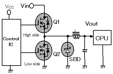
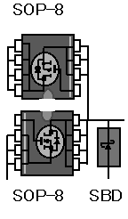
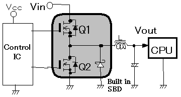
| < Configuration Diagrams > |
- Conventional configuration using 3 packages
|
 |
 |
| |
|
- HAT2180RP Composite power MOSFET
|
|
 |
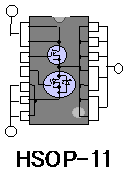 |
* Q1: Power MOSFET for the high-side switch ,Q2: Power MOSFET for the low-side switch,
SBD: Schottky barrier diode
|