
Hitachi
Contact InformationContact Information

    1. Semiconductor Device Trends and Diversifying Customer Needs in the IoT Era

    1. Semiconductor device trendsSemiconductor device trends

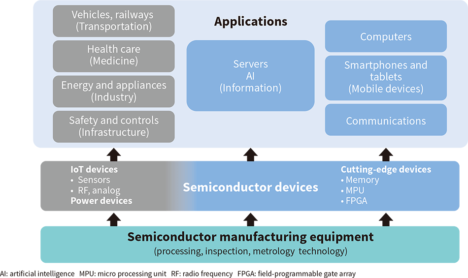
    With the rise of the Internet of Things (IoT), semiconductor devices are being incorporated into all types of devices, with a wider range of applications, not only for smartphones and personal computers, but also for sensing, communications, big data processing, data storage, and more. Demand for these devices is also steadily increasing. Materials and architecture are steadily evolving to improve the performance of, not only cutting-edge memory and logic devices, but also power semiconductor devices and various types of sensors.

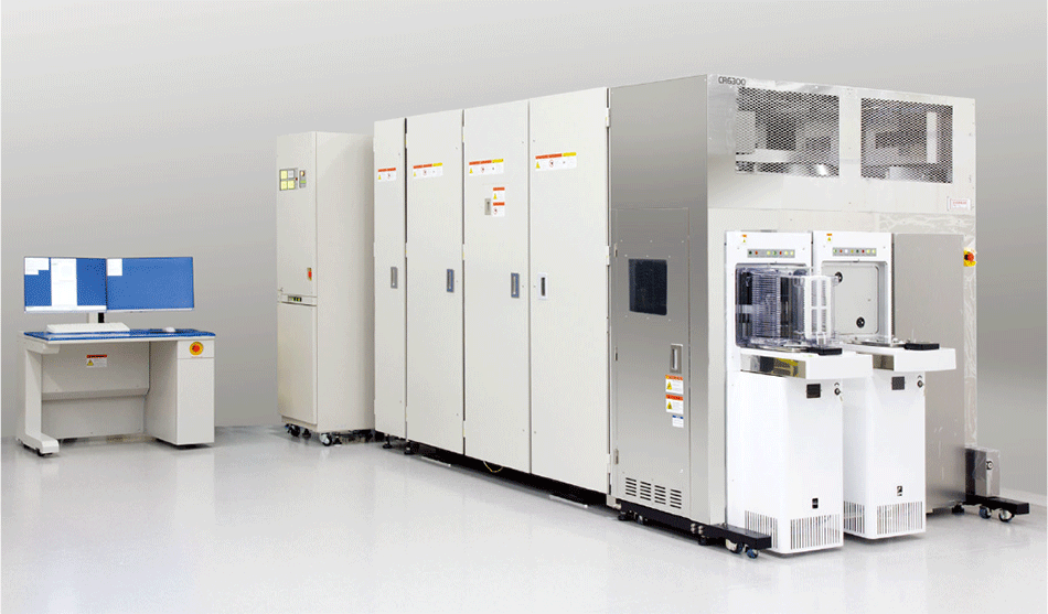
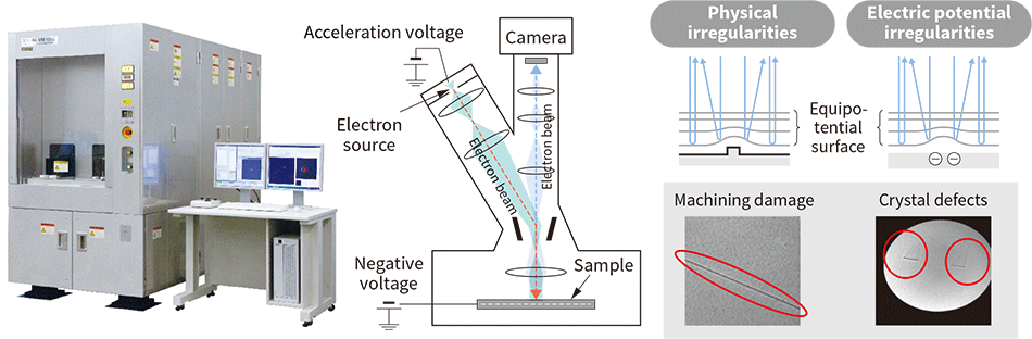
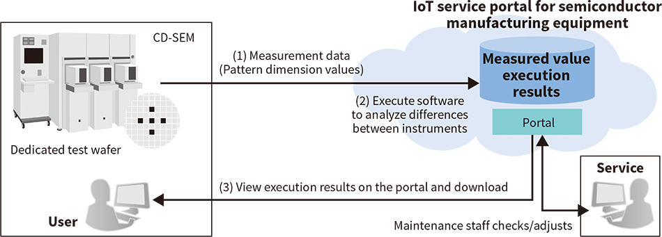
    Customer needs are also changing for semiconductor device manufacturing equipment. For example, the miniaturization and increasingly complex structure of cutting-edge devices makes it more difficult to process them into the shapes as designed. The many points where the designed pattern shapes differ from the actual patterned dimensions in complex fabrication processes need to be measured and checked. For next-generation power semiconductors such as silicon carbide (SiC), techniques for non-destructive inspection of wafer substrates are needed to reduce crystal defects. At the same time, in order to consistently manufacture high-performance devices, steps must be taken to reduce differences among the several metrology tools used in the semiconductor manufacturing process, so that every tool reports the same results.

    The Hitachi Group will continue to provide technology and solutions to meet these diverse customer needs.

    (Hitachi High-Technologies Corporation)

    2. Review SEM Shortening the Development Time of Semiconductor Devices

    2. Review SEM CR6300Review SEM CR6300

    At each stage from semiconductor device development to mass production, it is essential now to obtain and evaluate vast amounts of high-resolution images of defects that occur in manufacturing process in order to quickly spot processes where failures are present. Hitachi developed the high-speed, highly functional review scanning electron microscope (SEM) CR6300 to meet this demand.

    The CR6300 is designed with an improved wafer stage to speed up processing, and also has an electron beam control system that is linked to the stage's movement to stabilize images, tripling throughput (to 21,000 points per hour) compared to conventional technology. It incorporates six types of detectors to sort out secondary electrons (SE)*1 and backscattered electrons (BSE)*2 (electron signals generated by electron beam irradiation of samples) based on their emission angle and energy, improving the capture rate of signal electrons emitted from deep trenches and contact holes with high aspect ratios, enhancing the ability to observe and evaluate pattern shapes.

    The review SEM is also equipped with a function that statistically evaluates shape differences between the pattern layout design data of the semiconductor device and the actually processed patterns, shortening the time required to optimize the processing conditions of semiconductor fabrication equipment.

    (Hitachi High-Technologies Corporation)

    *1
    Electrons emitted from inside the sample when its atoms collide with primary electrons.
    *2
    The portion of primary electrons that are reflected off the surface of the sample when they collide with atoms.

    3. Mirror Electron Inspection System for the Next-generation Power Device Market

    Power devices that use wide bandgap semiconductors [like SiC and gallium nitride (GaN)] are attracting high expectation due to their low power loss. Currently, they are being used in consumer products, photovoltaic power generation equipment, and rolling stock, their market is expected to expand even more to electric vehicles and the like by 2020. However, crystal defects in SiC epitaxial wafers and bulk wafer machining damage often cause low yield and poor reliability, challenges that are driving prices up.

    As a solution to these issues, Hitachi developed and productized an electron mirror inspection system that can non-destructively detect crystal defects in wafers and machining damage. This system is based on electron microscopes, a core technology of Hitachi, and works under a new concept. Electron beams fired at samples bounce back due to the electrostatic potential directly above the evaluation sample. These electrons are captured as signals by the top detector to form a detection pattern. The system can detect crystal defects and machining damage without letting the electron beam penetrate into the sample, and can also be used for wafer shipment inspection.

    The main features are as follows.

    1. Uses a mirror electron optical system
    2. Non-destructive inspection of epitaxial wafer stacking faults, and basal plane dislocation, and threading dislocation
    3. Non-destructive inspection of bulk wafer machining damage (latent flaws or scratches), stacking faults, basal plane dislocation

    (Hitachi High-Technologies Corporation)

    3. Mirror electron inspection system Mirelis VM1000 (left), instrument architecture (middle), and image formation principles (right)Mirror electron inspection system Mirelis VM1000 (left), instrument architecture (middle), and image formation principles (right)

    4. Service Solution to Reduce Variation between CD-SEM

    Critical dimension-scanning electron microscopes (CD-SEM) are often used on the semiconductor device manufacturing line to make sure the pattern dimensions are processed as designed. In recent years, demand has grown to reduce measurement variations among multiple CD-SEMs to the sub-nanometer level.

    Hitachi has leveraged its long track record in supplying CD-SEM over many years to begin providing a new service named Innovative Matching Precision Activity (IMPAct). This service minimizes variations in the installation environment for older models (the S-9380II and CG4000 Series), and monitors them to maintain a stable status. IMPAct calibrates already-installed instruments by measuring the patterns on dedicated test wafers, reducing measurement variations between CD-SEMs. After calibration, checks are made via measurements at regular intervals. The measurement data is sent to a dedicated portal website to allow fully automatic visualization of differences in measurement values between CD-SEMs and resolution. Causes of instrument fluctuations are quickly pinpointed to shorten the time required to take action.

    (Hitachi High-Technologies Corporation)

    4. System architecture of the IoT remote monitoring service by IMPActSystem architecture of the IoT remote monitoring service by IMPAct

    Download Adobe Reader
    In order to read a PDF file, you need to have Adobe® Reader® installed in your computer.