
|
 News releases News releases |
|
|
|
 PDF Download(PDF Type, 80Kbyte) PDF Download(PDF Type, 80Kbyte) |
|
| June 1, 2005 |
|
| Hitachi and Renesas Technology Develop Through-Hole Electrode Technology to Enable Interconnection of Stacked Chips at Room Temperature |
|
| - The new technology enables a room-temperature bonding of 10 stacked chip layers in a package with a thickness of 1 mm or less - |
|
|
 |
|
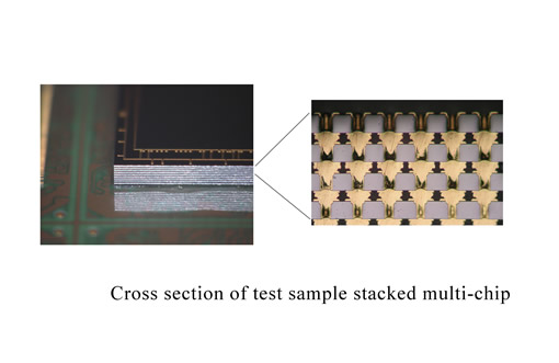
Tokyo, June 1, 2005 --- Hitachi, Ltd. (NYSE:HIT / TSE: 6501) and Renesas Technology Corp. today announced a new stacked chip technology that uses a through-hole interconnection method to enable chips to bond at room temperature. The new technology eliminates the need for wire bonding and reduces package thickness by more than 60% for the most advanced SiP (System in Package) products. The method offers a new packaging technology option for developing 3D-stacked SiP products.
With this new packaging technique, LSI chips that are between 30 and 50 µm thick are fashioned with through-hole electrodes between the top and bottom sides and gold stud bumps. It then allows the bumps and through-hole electrodes to connect by applying a compressive force at room temperature.
Details of this new technology will be presented at Electronic Components and Technology Conference 2005 (ECTC 2005) being held in Lake Buena Vista, Florida, U.S.A. from May 31, 2005.
Using this technology, the package thickness of a two-layer SiP is reduced by 60% or more, from the current 1.25 mm to 0.5 mm or less. It also enables a package thickness of 1 mm or less to be achieved when stacking 10 LSI chip layers. In addition, chip-to-chip interconnection is performed at room temperature to simplify the manufacturing process.
The chip-stacking technology has several advantages over current stacking methods. Today most SiP products achieve electrical interconnection between chips using wire bonding, but the need to provide wire space limits package thickness. Also, since chip-to-chip connections are made via package substrate wiring, the number of package substrate layers increases, leading to higher substrate costs. In addition, the longer wiring required for connecting stacked chips causes lower performance. The new technology eliminates these issues for chip-to-chip bonding and will allow future SiP products to be made smaller and thinner, while offering higher speed and larger capacity.
Features of the newly developed technology are as follows:
| (1) |
Room temperature chip-to-chip interconnection using caulking1 technique |
|
For chip-to-chip interconnection, a mechanical caulking operation is used that makes use of the plasticity of gold stud bumps. This enables the gold stud bumps and through-holes to be interconnected electrically at room temperature simply by applying force. This bonding technique can also be used for room-temperature connection between a chip and substrate. While conventional through-hole electrode (interconnection) techniques using solder or similar metallic bumps require high-temperature bonding, this new technology simplifies the manufacturing process by enabling bonding at room temperature. |
| (2) |
Through-hole electrode formation on back-side of wafer by means of a low-temperature process |
|
Through-hole electrodes are formed on the back-side of a wafer as thin as 30 to 50 µm. As these through-hole electrodes are fixed to the glass wafer with a removable adhesive, they must be formed at a temperature lower than the maximum temperature that the adhesive can withstand. With this new process, the etching and film-forming occurs at a temperature less than half that previously required (less than 150°C). Furthermore, the breakdown voltage between the through-holes attains the same level as inside the LSIs. |
| Notes |
| 1) |
Caulking: Making a firm connection by using differences in deformation between materials. |
|
|
|
| Information contained in this news release is current as of the date of the press announcement, but may be subject to change without prior notice. |
|
|
 |
PDF files are in Adobe's Portable Document Format. To view them you need Adobe(R) Reader(R) by Adobe Systems Incorporated. |
|
|
|
|
|