Hitachi, Ltd. (NYSE:HIT) today announced the HD66324S driver for XGA-size*1 large-screen, high-
definition TFT liquid crystal displays, which reduces output voltage deviation to +/- 1 mV through the use of
Hitachi's proprietary offset cancellation circuit. Sample shipments will begin from December 1998 in Japan.
The HD66324S provides a high-quality, flicker-free display, while at the same time achieving about 25%
lower power consumption than previous Hitachi models.
Notebook PCs and space-saving desktop PCs and monitors equipped with a TFT panel are growing in
popularity, bringing a growing demand for larger XGA- and SXGA-size*2 screens that offer higher
definition. In line with this trend, we can expect to see an increasing demand for special-purpose drivers to
drive the vertical data lines of high-definition TFT panels.
Hitachi has previously released the HD66322 384-output, dot-inversion type driver for XGA-size color TFT
liquid crystal displays, but with the increasing size and definition of TFT panels, a need has arisen for data
line drivers offering high drive capability to handle the panel load, together with output voltage uniformity
and lower power consumption.
In response to this need, Hitachi is now releasing the HD66324S, offering reduced output voltage deviation
and lower power consumption.
The HD66324S is a data line driver suitable for use with XGA-size large-screen, high-definition color TFT
displays. This driver accepts 6-bit digital data per pixel, generates voltages for 64 gradations, and provides a
260,000-color display. With 384 outputs incorporating 384 6-bit D/A converters and op-amps, XGA data
line drive can be handled by eight HD66324S drivers.
One important characteristic of a data line driver is output voltage uniformity. With previous models,
deviation in the input/output offset voltages of the 384 op-amps incorporated into the same chip resulted in a
drive voltage deviation of around +/- 10 mV. This new driver, however, employs a proprietary offset
cancellation method whereby the input/output offset voltage polarity can be reversed between frames,
enabling drive voltage deviation to be kept to +/- 1 mV. This results in a high-quality, flicker-free panel
display.
In addition, as a means of reducing chip area and power consumption, an improved paired-amp system is
used in which op-amp circuits are shared between adjacent outputs, resulting in an about 20% smaller chip
area and approximately 25% lower power consumption than the previous HD66322.
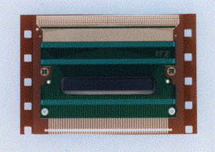
With the use of a TCP*3 package, employing 44  m pitch technology for the inner leads, the design of the
HD66324S minimizes both chip area and package area.
Future plans call for an enhanced product lineup attuned to the trends in TFT panel displays, based on the
newly developed offset cancellation drive circuit, together with the paired-amp system and multi-pin
technology.
Notes:1.XGA (Extended Graphic Array): XGA is an IBM standard, with a display comprising 1024x
768 dots.
2.SXGA (Super Extended Graphic Array): SXGA is a high-definition display standard, with a
display comprising 1280x1024 dots.
3.TCP (Tape Carrier Package): A package mounted on a thin-film tape, allowing ultra-thin type
mounting (1 mm or less).
<Typical Applications>
TFT panel applications
- Notebook PCs
- Space-saving desktop PCs
- Monitors
<Prices in Japan> (For Reference Only) m pitch technology for the inner leads, the design of the
HD66324S minimizes both chip area and package area.
Future plans call for an enhanced product lineup attuned to the trends in TFT panel displays, based on the
newly developed offset cancellation drive circuit, together with the paired-amp system and multi-pin
technology.
Notes:1.XGA (Extended Graphic Array): XGA is an IBM standard, with a display comprising 1024x
768 dots.
2.SXGA (Super Extended Graphic Array): SXGA is a high-definition display standard, with a
display comprising 1280x1024 dots.
3.TCP (Tape Carrier Package): A package mounted on a thin-film tape, allowing ultra-thin type
mounting (1 mm or less).
<Typical Applications>
TFT panel applications
- Notebook PCs
- Space-saving desktop PCs
- Monitors
<Prices in Japan> (For Reference Only)
| Product Code | HD66324S |
| Sample Price (Yen) | 800 |
 [ Supplementary Information ]

< Specifications >
|
Item |
Specification |
|
Function |
64-gradation TFT driver data line driver |
|
Power supply voltage |
3.0 to 3.6 V (logic)
6.0 to 11.0 V (analog) |
|
Operating temperature |
-20 to 75 degrees C |
|
Package |
443-pin TCP |
|
Data input |
36-bit digital input (6 bitsx 6 pixels) |
|
Drive outputs |
384 outputs |
|
Output voltage accuracy |
+/- mW (when using offset cancellation) |
|
Data line charge time |
7 micron S |
|
Clock speed |
45 MHz |
|
Other functions |
Offset cancellation
Dot inversion function
N-line inversion function
Data inversion function |
|