
Hitachi
Contact InformationContact Information

    1. Technological Trends in Advanced Devices and Diversity of Customer Requirements

    Progress in end products such as smartphones, servers, automobiles and robots is driven by improvements in the performance of semiconductor devices. These improvements have been achieved not only through miniaturization but also by the introduction of three-dimensional structures and new types of memory.

    The current device generation will shift to 7 nm and less, thanks to the adoption of multiple patterning technology and extreme ultraviolet (EUV) lithography. On the other hand, production volumes of 3D-NAND flash memory that vertically stacks memory cells are increasing and the number of stacks is expected to reach 100 layers in a few years. A number of new materials such as SiGe (silicon germanium) are being examined for the channel material of the fin-shaped field effect transistor, which is used in high-performance logic processors. In the case of new memory, magnetoresistive random access memory (MRAM) has moved a step ahead of other types of memory with its high access speed, data retention and endurance. MRAM is set to shift from the development stage to the mass production stage.

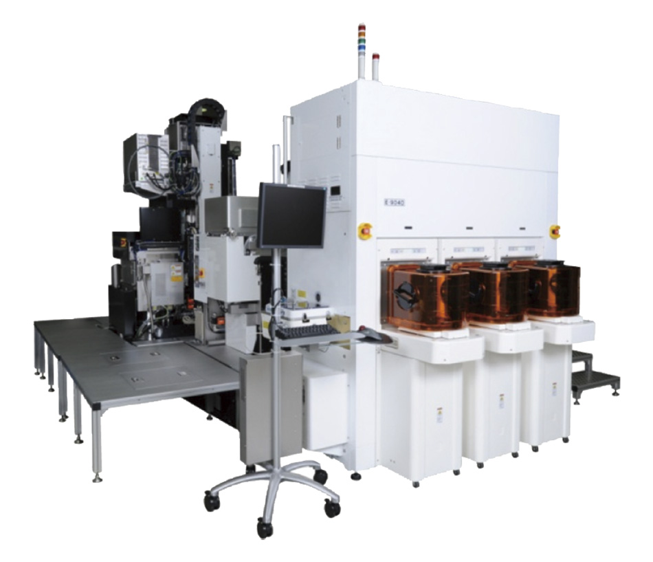
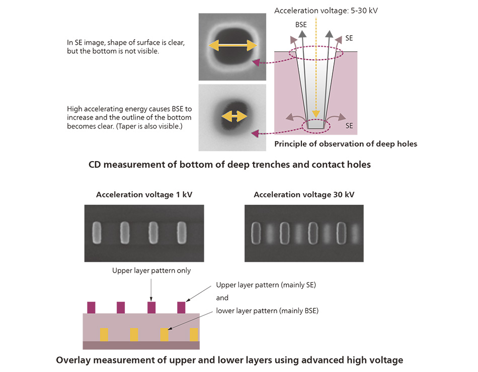
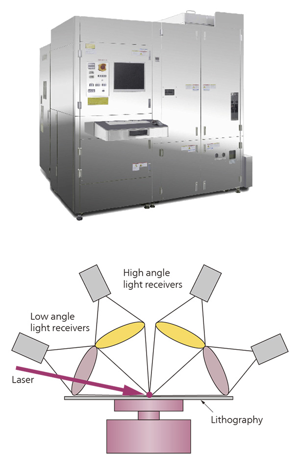
    Customer needs are also changing in response to these technological trends. In addition to existing technologies, control of critical particles/defects in the EUV lithography process, high-precision processing and metrology for MRAM and new materials are required. Technologies for etching and critical dimension measurement for deep trenches and holes are also important in 3D-NAND memory manufacturing.

    Hitachi Group continues to provide advanced technologies and solutions that satisfy these diversified customer needs.

    (Hitachi High Technologies Corporation)

    1. Technological trends in advanced devices

    2. Plasma Etching System for MRAM Fabrication in Vacuum Processing

    2. Plasma etching system E-9000 series for MRAM fabrication

    There are high expectations for the future use of MRAM as non-volatile memory due to the excellent device characteristics of MRAM elements. However, mass production of MRAM was considered difficult from the viewpoint of damage to the MRAM elements during etching and the stability of mass production.

    Hitachi has now developed the E-9000 series for MRAM fabrication in vacuum processing. The main units built into the system are as follows.

    1. Electromagnetically coupled plasma (EMCP) etching unit with unique cleaning components.
    2. Post etch treatment (PET) unit for the purpose of restoring device performance.
    3. Low-temperature plasma chemical vapor deposition (CVD) unit for forming a high moisture-proof protection film.

    Through the use of the proven and tested EMCP unit for engraving non-volatile material etching to ensure the stability of mass production and the PET unit’s damage recovery technologies, the E-9000 series is expected to be put into mass production for the first time for 300 mm wafers. The E-9000 series can also be customized to meet increasingly diverse customer needs through the addition of up to nine linkable units.

    (Hitachi High Technologies Corporation)

    3. Advanced High Voltage CD-SEM for Deep Trenches and Holes

    In semiconductor device manufacturing technology, the introduction of 3D and high aspect ratio construction as seen in 3D-NAND devices has given rise to increased demand not only for improvement in the precision of dimensions associated with miniaturization but also for measurement of the dimensions of deep trenches and contact holes, and for overlay measurements of the actual device patterns. To meet this demand, Hitachi developed the advanced high voltage critical dimension-scanning electron microscope (CD-SEM); CV5000 series, which is capable of measuring actual device patterns.

    The advanced high voltage CD-SEM; CV5000 series is the first semiconductor SEM series to be fitted with a 30 kV electron gun. By detecting secondary electrons (SE*1) and backscattered electrons (BSE*2) emitted from a sample, the advanced high voltage CD-SEM; CV5000 series can measure the bottom of deep trenches and contact holes, and can also perform high precision overlay measurements of device patterns through insulator films. Especially when measuring the deep trenches and contact holes typical of 3D-NAND, CV5000 series uses high energy BSE detection to measure the dimensions of deep trenches more than 3 μm. As for overlay measurements, CV5000 series can measure actual device patterns that could not be measured with existing optical overlay devices, and achieve 0.3 nm or less in measurement accuracy and repeatability.

    (Hitachi High Technologies Corporation)

    3. Measurement of actual device pattern by advanced high voltage CD-SEM

    *1
    SE (secondary electron): An electron that is emitted from a material upon being irradiated by an electron beam.
    *2
    BSE (back scattering electron): A beam electron that is reflected backward.

    4. Wafer Surface Inspection System for EUV Lithography

    4. Wafer surface inspection system LS9300A (top) and structure of multi-detector light receiver (bottom)

    Various new materials and new processes are being examined, with a view of adopting EUV lithography for volume production. Hitachi has now developed the LS9300A wafer surface inspection system, which is capable of detecting defects specific to the EUV process at high speed and with high sensitivity, to support development of the EUV process and to maintain a high yield during mass production.

    The LS9300A is a laser scanning-type inspection device that detects defects by capturing the light scattered from defects. The defects that occur in the EUV process are unlike other foreign particles caused by wafer transfer and have high directivity to the light scattered from defects. The LS9300A employs Hitachi’s proprietary multi-detector configuration to efficiently capture the light scattered from defects unique to the EUV process and achieve highly sensitive inspection.

    Also in bare wafer inspections, which are used as the standard procedure in tool monitoring, the LS9300A employs a high output laser and newly developed high sensitivity sensor to achieve a maximum sensitivity of 19 nm, which is four times higher than existing models.

    Through EUV process technology and technology to increase sensitivity, the LS9300A will continue to help customers develop the EUV process and maintain yield.

    (Hitachi High Technologies Corporation)

    Download Adobe Reader
    In order to read a PDF file, you need to have Adobe® Reader® installed in your computer.