Solutions Based on Measurement Technology
Next Generation of New Materials Development Based on Large Datasets
Materials informatics, the recursive extraction of correlations and other rules on material properties from large datasets, has attracted attention for its potential in the development of highly efficient new materials. Because microstructure is an intermediate factor that links the production recipe for a material to its properties, providing a view into aspects of microstructure not accessible to past techniques is one of the challenges of measurement technology. To quantify the interpretation of measured data, which has been done by experts with domain knowledge of materials, and to unify the yardsticks of microstructure are also vital to the integration of informatics with measurement technology. This article describes techniques for measuring material properties at the nano-scale and for extracting feature values from electron microscope images, work that Hitachi is doing to improve the efficiency of materials development.


As global challenges such as rising populations, resource depletion, and climate change feed off each other and become increasingly severe, high expectations are being placed on the materials industries underpinning the infrastructure and goods that provide the basis of the economy and people's way of life. Materials informatics is a way of improving the efficiency of materials development that works through the recursive extraction of correlations and other rules on material performance from large quantities of systematically collected data. The technique has started to produce results, such as using a combination of numerical calculations and data science to predict optimal material compositions(1), and it is entering practical use in the materials search phase of the development process. Hitachi has proceeded with efficient materials search with simulation combined with response surface methodology in the selection of additive elements for lead-free solder, etc.(2).
Unfortunately, as the use of simulation for prediction can prove difficult in materials development that also involves a production process, an experimental approach based on prototyping and measurement is needed. This frequently involves experts working through a process of trial and error to find the best possible solution given constraints that include time, cost, and experimental conditions. As a result, materials development not only takes a long time, it is also highly dependent on the people involved, requiring knowledge and many years of experience. Given the increasing diversity and complexity of the properties required for materials and the production processes for achieving them, more efficient materials development is expected by combining an experimental method and informatics.
In materials development, not only objective characteristics such as mechanical, electrical, and magnetic characteristics, but also the measurement of microstructures has been utilized. Examples include the use of X-ray diffraction on plastics to determine whether the material is crystalline and its crystal structure, and the use of electron microscopes on metals to look at their grain structure, precipitates, crystal defects, crystal dislocations, and other features. These measurements provide feedback to the production recipe (material composition and process parameters) to help achieve the desired properties. This is because the microstructure is an intermediate factor that bridges a production recipe and the material's performance such that a direction or policy for obtaining objective characteristics can be obtained through the understanding of the microstructure. Accordingly, providing a view into aspects of microstructure not viewable by past technologies is one of the challenges for measurement technology in seeking to improve the efficiency of materials development. While surface analysis to visualize elements and chemical states is already in widespread use, other requirements include ways of visualizing physical characteristics such as electrical and magnetic characteristics as well as measuring their dynamic changes.
In data analysis, a key question is how to extract feature values that are correlated with material performance from measurements such as images or spectrums. Whereas the interpretation of measurement data is currently a job for experts with domain knowledge of materials and measurement, automating and quantifying this task would go a long way toward making informatics part of the process.
The following sections describe technologies for measuring material properties at the nano-scale and for extracting feature values from electron microscope images, work that Hitachi is doing for more efficient materials development.
Ferromagnetic substances, represented by magnets and iron, are considered groups of tiny regions with magnetic moments produced by atomic electron spins facing the same direction. These regions that act like small magnets are called magnetic domains. Controlling the arrangement of these magnetic domains is key to improving the performance of magnets such as those used in electric motors and magnetic recording media.
Spin-polarized scanning electron microscopes (spin SEMs) are a technique to produce an image of the micro-scale magnetization distribution by measuring the spin polarities of electrons in a ferromagnetic substance sample. Figure 1 shows how a spin SEM works. When a finely focused primary electron beam is irradiated at the surface of a sample, if it is a ferromagnetic substance, the atoms that make up the sample emit secondary electrons while the direction of the spins is the same. A spin SEM detects the spin polarity of secondary electrons, which are emitted by making use of the above phenomenon, and maps them to obtain magnetic domain images(3).
Figure 1—Principle of Spin SEM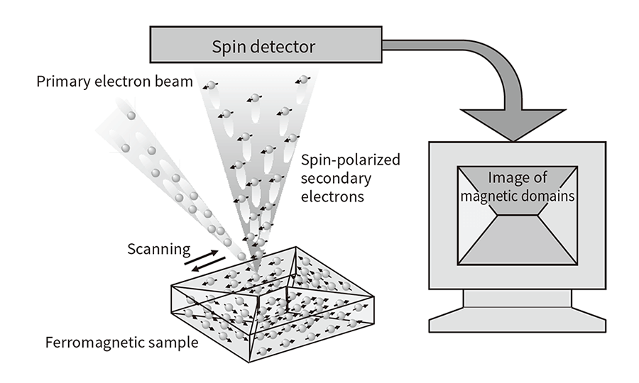 A spin-polarized scanning electron microscope (spin SEM) irradiates a finely focused primary electron beam at the surface of a sample and detects the spin polarization of secondary electrons emitted from inside the sample. By mapping the magnitude and orientation of spin polarization, the micro-level magnetic domain in the sample is visualized.
This section introduces the evaluation of magnetism in the grain boundary phase of an Nd-Fe-B sintered magnet by using a spin SEM. This magnet has very high coercivity and saturation magnetization and is used in a variety of fields including motors and generators. As a major factor that significantly affects the coercivity of Nd-Fe-B sintered magnets, the magnetism in the grain boundary phase has gained attention. This phase is about 2 nm thick and sandwiched between crystal grains of several micrometers with the saturation magnetization consisting of a 1.6 T-level main phase. In order to measure the above grain boundary phase without being affected by the main phase and atmospheric oxidation, Hitachi developed a method to sequentially measure changes in spin SEM images while fracturing a sample inside a vacuum chamber of the spin SEM (see Figure 2) and then shaving the surface of the sample by argon ion milling every several tens of nanometers.
Figure 3 (a) and Figure 3 (b) show spin SEM images of Nd-Fe-B sintered magnets in a demagnetized state immediately after fracture in a vacuum chamber and after argon ion milling. The oriented direction components (horizontal direction) of the spin polarizations are indicated by the grayscale gradations. The spin SEM image immediately after the fracture shows a strong contrast only in the center while the image after the argon ion milling shows a strong contrast as a whole. This result indicates that, shortly after fracturing, the surface of the sample is covered by a grain boundary phase with low level of magnetization and only part of it (the dotted circle) exposes the main phase due to fracture inside the grain. Also indicated is that the argon ion milling removed the approximately 2 nm grain boundary phase to expose the main phase on the surface, and magnetization images of several magnetic domains that are in an antiparallel state to each other were observed in strong contrast. This interpretation is also supported by micro-auger measurements conducted by exploiting localized presence of copper in the grain boundary phase. Hitachi succeeded in a quantitative measurement of magnetization in the grain boundary phase using this technique. As a result, it was understood that the grain boundary phase of Nd-Fe-B sintered magnets, though weaker than the main phase, has sufficient magnetization to be considered ferromagnetic(4).
Figure 2—How to Observe Fracture Surface of Nd-Fe-B Sintered Magnet with Spin SEM Since the grain boundary phase in Nd-Fe-B (neodymium-iron-boron) sintered magnets is so prone to oxidation, samples are first fractured inside the sample chamber (vacuum) of the spin SEM and the magnetization of the surface is measured. Then, by repeating magnetization measurement while shaving the surface of the sample by argon ion milling every several tens of nanometers, the magnetization of the grain boundary phase can be quantitatively measured.
Figure 3—Spin SEM Image of Nd-Fe-B Sintered Magnet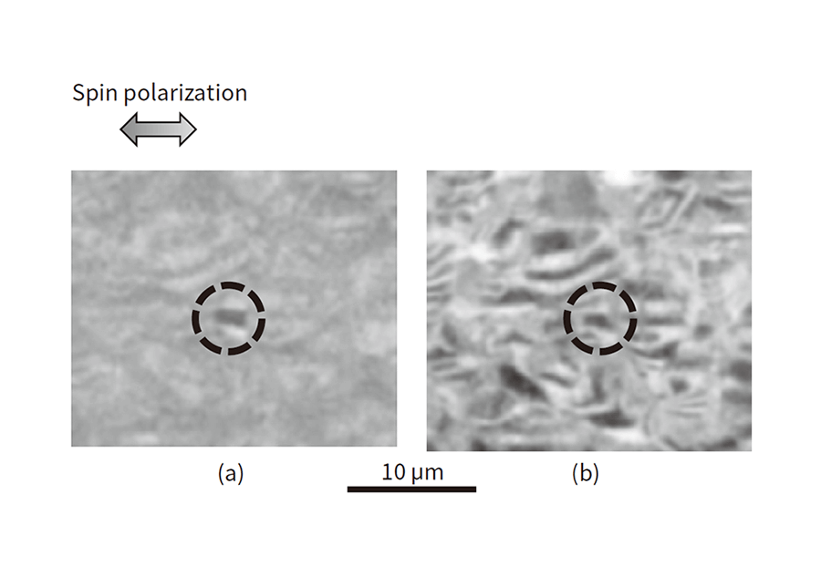 Image (a) shows the surface immediately after fracturing. The only region of high contrast is in the dotted circle in the middle of the image. Image
(b) shows the surface after argon ion milling. Contrast is strong as a whole.
As for metal materials, which are used as structural materials, it is known that their microstructures are strongly correlated with performance, and microstructures have long been observed with electron microscopes. Recently, electron back-scattered diffraction pattern (EBSP) analysis, in which an electron beam is irradiated at a sample tilted in a SEM chamber and diffraction patterns that occur are measured with a special detector, has widely been utilized. One of the reasons why EBSP is used despite its longer imaging time and the need for careful sample preparation due to the sensitivity of a sample's surface condition is that microstructure features such as crystal types and the sizes and shapes of crystal grains can be quantitatively known via the analysis.
However, contrast due to crystal orientation, mean atomic number, and shape is also contained in backscattered electron (BSE) images that can be obtained using a conventional electronic microscope without needing a special detector. A highly skilled electronic microscope user estimates boundaries between different crystal grains and crystal structures from complicated image contrast. Automating and quantifying this process has the potential to provide large quantities of information with BSE images, which take several tens of seconds for imaging and can be captured in high volumes.
Accordingly, Hitachi worked on systematic analysis of microstructures using BSE images. The subject matter, the microstructure of chromium-based duplex alloy consists of α and γ phases as shown in Figure 4, and a microstructure called a dendrite is formed in the α phase. As the α and γ phases have different densities, a difference of brightness (Z contrast) resulting from the difference in the mean atomic numbers appears in BSE images. On the other hand, even α phases have different brightness. This makes it impossible to differentiate between the α and γ phases using conventional image processing. Therefore, supervised learning was chosen as a way to perform phase identification.
Figure 5 shows a flowchart of the phase identification. Users define how to identify a correct phase for a particular region of an acquired image. In this example, label data is created to designate whether it should be identified as α phase, γ phase, or dendrite per pixel. The network reads the original BSE image and labeled data as a learning dataset so as to create a learning model. By using this, a lot of images can be automatically and quantitatively identified.
Figure 4—BSE Image of Chromium-based Duplex Alloy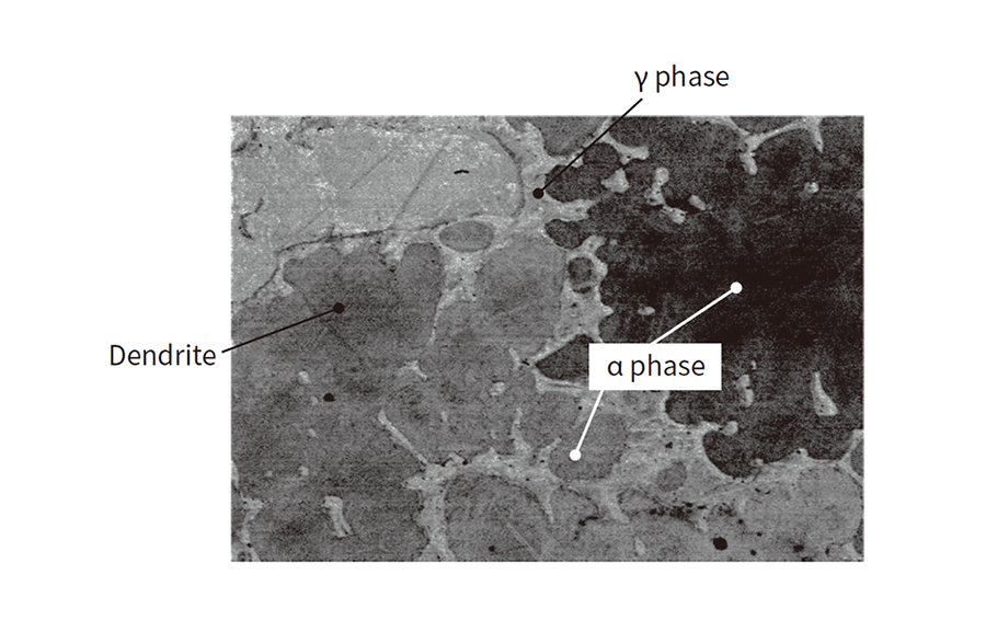 The backscattered electron (BSE) image of a chromium-based duplex alloy mainly consists of α and γ phases with different crystal structures, and a microstructure called a dendrite is formed in the α phase. α phases vary in terms of brightness due to their differences in crystals.
Figure 5—Flowchart of Phase Identification Using Supervised Machine Learning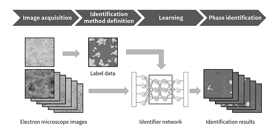 The user defines how to identify the correct phase for a particular region of an acquired image. An identifier network is created with pairs of original BSE images and their label data as learning data. Finally, a lot of images are automatically and quantitatively identified using this identifier network.
Figure 6—Feature Values Extracted from Electron Microscope Images and Model of Correlation with Vickers Hardness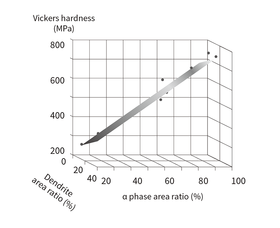 Of the candidate feature values extracted from electron microscope images, the ones that were strongly correlated with Vickers hardness were the α phase area ratio and the proportion of dendrites. According to the model formula created using these feature values, the measured Vickers hardness can be forecasted within an error of 10%.
According to the identification results from machine learning, a variety of feature value candidates can be calculated. These include size-related feature values such as the size, area ratio, and length of circumference of each region, as well as shape-related values such as profile ratio and circularity. It is important to extract those feature values related to material performance and study correlation with the material performance for looking for a best solution to achieve the targeted material performance.
It was understood that if the performance indicator for chromium-based duplex alloy is Vickers hardness, the feature value highly correlated with this is α phase's area ratio and the proportion of dendrites present in the α phase. Using these two feature values, a model formula was created to forecast Vickers hardness and the result is shown in Figure 6. It was observed that the difference between the value predicted with the above model formula and measured Vickers hardness is within 10%(5).
This article introduced spin SEMs, which measure and visualize nano-scale physical properties, and a technique for extracting microstructure feature values from electron microscope images that adopt machine learning, in order to improve the efficiency of materials development based on experiments.
It is thought that further advances in informatics-based materials development will require a variety of initiatives beyond those described above. First of all, it is more and more important to know 3-dimensional microstructures. For instance, in tire development, the degradation of the adhesive interface between rubber and steel cords has been understood three-dimensionally and composition changes due to the degradation have been successfully analyzed, thanks to the combination of focused ion beam (FIB) – SEM composite instruments and image processing technologies(6). It is also important to integrate and organize materials-related data. Hitachi has managed multidimensional arrays such as experiment data and value simulation data, and developed visualization systems(7). More systematic data collection and analysis making use of these systems is expected. In coordination with these trends, Hitachi plans to continue working to fuse the development of measurement technologies and informatics.
