World-leading Measuring Instruments and Systems
SiC power devices capable of significant power loss reductions have started to be used in mobility systems such as automotive and rail systems. But since the SiC wafers used as the substrate contain various crystal defects, these SiC power devices will require further technology development before they can come into widespread use. The Mirelis VM1000 is an inspection system that uses mirror electron microscope technology to enable nondestructive detection of previously undetectable SiC wafer polishing damage and crystal defects (basal plane dislocations). It can assist technology development designed to improve SiC wafer processing procedures and device reliability. This article presents Mirelis VM1000’s defect detection principle and equipment specifications, along with some inspection examples.


Reducing power loss is an important key to achieving the ultrasmart world described in the Society 5.0 vision for the future set forth by the Japanese government. Power devices used for power conversion and step-up/step-down voltage transformation are key devices for saving energy. Power devices made from silicon (Si) materials are currently the mainstream type used, but developers have recently been working on silicon carbide (SiC) power devices made from SiC materials that can reduce power loss up to 50%(1). Their use has begun in air conditioner and solar power generation power conditioners, along with rail and automotive applications(2). But the widespread rise of SiC power devices has been impeded by factors such as their high cost relative to Si power devices(3), and SiC wafers also contain various crystal defects(1) that are an obstacle to improving device manufacturing yield.
SiC wafers are cut from an SiC ingot, subjected to mechanical polishing and chemical mechanical polishing (CMP), and then shipped to the market as bulk wafers. Devices are manufactured by forming an epitaxial film on the bulk wafer. Device manufacturers either handle the epitaxial film formation in-house, or purchase wafers with a ready-made epitaxial film (epi wafers) from wafer manufacturers. So SiC wafers come in bulk and epi types, and the defects that lower quality are different in each. Unlike Si wafers, SiC wafers have large numbers and types of defects. Among these defects, the types shown in Figure 1 are thought to affect device manufacturing yield and reliability(1), (4), (5).
Bulk wafer defects include processing damage (such as scratches and latent scratches) caused during ingot cutting or any number of multiple polishing procedures(4), along with basal plane dislocations (BPDs)(1) inherently present in the ingot. Processing damage generates unevenness and defects in the surface during epitaxial film formation, degrading epi wafer quality. BPDs propagate to the epi layer, expanding stacking faults through electrical conduction during device operation, and causing conductivity deterioration that increases diode resistance during the ON state(5). Epi wafers have large critical defects (carrot defects, triangular defects, stacking faults, and downfall defects)(6) that can be as large as several hundred microns, and cause initial failures in devices. There are also threading dislocations(1)—crystal defects orthogonal to the basal plane with types such as threading screw dislocations (TSDs) and threading edge dislocations (TEDs). These defects are thought to affect reliability through issues such as device current leak(7).
Figure 1—Effects of Different Types of Defects on SiC Wafer Quality Shown here are the types of defects that need to be controlled in SiC bulk and epi wafers, and the typical adverse effects they have on wafer and device quality. It should be noted that the effects of crystal defects on device reliability have not been fully explicated.
The inspection methods currently in widespread use are optical inspections such as differential interference contrast microscopy, X-ray topography imaging using synchrotron facilities, photoluminescence, and the etch-pit method, which enables imaging using high-melting-point potassium hydroxide (KOH) etching to form pits. Table 1 lists the detection performance and features of these methods. The details of the principles of these technologies are beyond the scope of this article, so interested readers should refer to the relevant literature(1).
There are no nondestructive inspection technologies available on factory lines for processing damage and BPDs, both of which have major impacts on bulk wafer quality, so novel inspection methods are needed.
Table 1—Comparison of Detection Sensitivity for Defects of Interest Using Conventional Defect Detection Methods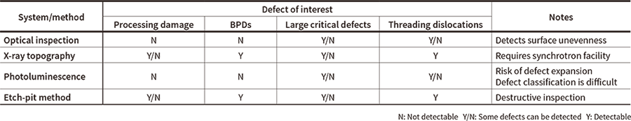 This table lists the technologies currently in use for detecting SiC wafer defects. “Optical inspection” includes systems that detect light diffusion and systems with differential interference contrast microscopes. These systems are for detecting unevenness in the wafer surface, but their sensitivity depends on their detection principle.
Differing from both scanning electron microscopes and transmission electron microscopes, mirror electron microscopes are, so to speak, the third type of electron microscope. This article will leave the details of explaining this technology up to the literature(8), (9), and instead focus on the role of mirror electron microscopes in SiC wafer defect detection. Figure 2 shows schematic diagrams of the optical system in a mirror electron microscope [see Figure 2 (a)], and the electron path in the neighborhood of the wafer surface [see Figure 2 (b) and Figure 2 (c)]. Figure 2 (a) also illustrates the ultraviolet irradiation optical system. The system emits ultraviolet radiation of higher energy than the band gap and uses it to charge the defects in the Si wafer(10).
The electron beams from the electron gun are brought together into a bundle of parallel electron beams by the irradiation electron optical system [see Figure 2 (a)], irradiating the wafer surface with an orthogonal and uniform-density distribution. An example of a defect-free SiC wafer surface is shown in Figure 2 (b). Since a negative voltage nearly equal to the electron gun's acceleration voltage is applied to the wafer surface, the irradiation electron beams decelerate before reaching the wafer surface, and the path is reversed by a surface of constant surface electrical potential (the equipotential surface). This phenomenon is called mirroring for its resemblance to the reflection of light by a mirror. Electron beams of uniform distribution are reversed orthogonally in relation to a flat wafer surface, pass through an imaging optical system [see Figure 2 (a)], and are imaged on a fluorescent plate, enabling a camera to photograph them as an image converted to visible light (the mirror electron image). When the mirror electron image is uniformly reflected as shown in Figure 2 (b), it becomes an image of uniform brightness without dark or light areas.
But when defects are present in the wafer surface [see Figure 2 (c)], the defect areas become locally charged by the ultraviolet radiation, resulting in a pattern of reflection that varies greatly. When the SiC wafer is an n-type wafer, the excited carriers (electrons) are captured, so the defect areas are charged negatively and the equipotential surface expands. The paths of these orthogonally-reflected electron beams are reversed by this expanded equipotential surface, but since the surface is not flat, the electron beams are reversed in a way that expands them. The density distributions of the reversed electron beams are no longer uniform and density decreases at the tops of the defects. As a result, dark images appear in mirror electron images formed by the imaging optical system, enabling the presence of defects to be detected(10)-(12).
Figure 3 shows examples of SiC wafer defect images detected by a mirror electron microscope. Figure 3 (a) is a bulk wafer latent scratch image. The crystal deformation within the wafer created during processing becomes charged, appearing as a black line. Figure 3 (b) is a bulk wafer BPD. The BPD is on the basal plane of an SiC crystal (tilted by 4 degrees in this wafer), so the portion near the surface appears as a black line due to the effect of the negative charge. The deeper the BPD becomes, the weaker the effect of the charge, and the lighter the black line becomes. Figure 3 (c) is an epi wafer stacking fault. This defect is also a defect in the basal plane, so the effect of the defect charge weakens as the basal surface deepens, lightening the defect image. Figure 3 (d) shows threading dislocation. This defect is a crystal defect that is orthogonal to the basal plane, so it takes the form of black spots. Mirror electron images show TSD defects as larger and blacker images than TED defects, enabling differentiation of these two defects.
As shown in Figure 2, defect detection by mirror electron microscope is made possible by drawing on contrast formation in the mirror electron image in response to unevenness in the equipotential surface on the wafer surface. There is no need for electron beam collision with the wafer surface. Accordingly, it is a completely nondestructive and noncontaminating inspection technology that enables inspections before wafer processing for device production. These benefits also make it an inspection technology suited to SiC wafer quality assessments.
Figure 2—Electro-optical System and Defect Detection Principle of Mirror Electron Microscopes As shown in (a), a mirror electron microscope uses a separator to bend electron beams passing through an irradiation optical system, and an electrostatic lens to collect them into a bundle of parallel electron beams that irradiate the wafer. Mirror electrons move through the separator, pass through the imaging optical system, and form an image on a fluorescent plate. Illustration (b) and (c) show the electron paths in the vicinity of an SiC wafer surface. Defects become negatively charged, greatly altering the mirror electron paths.
Figure 3—Mirror Electron Microscope Images of Crystal Defects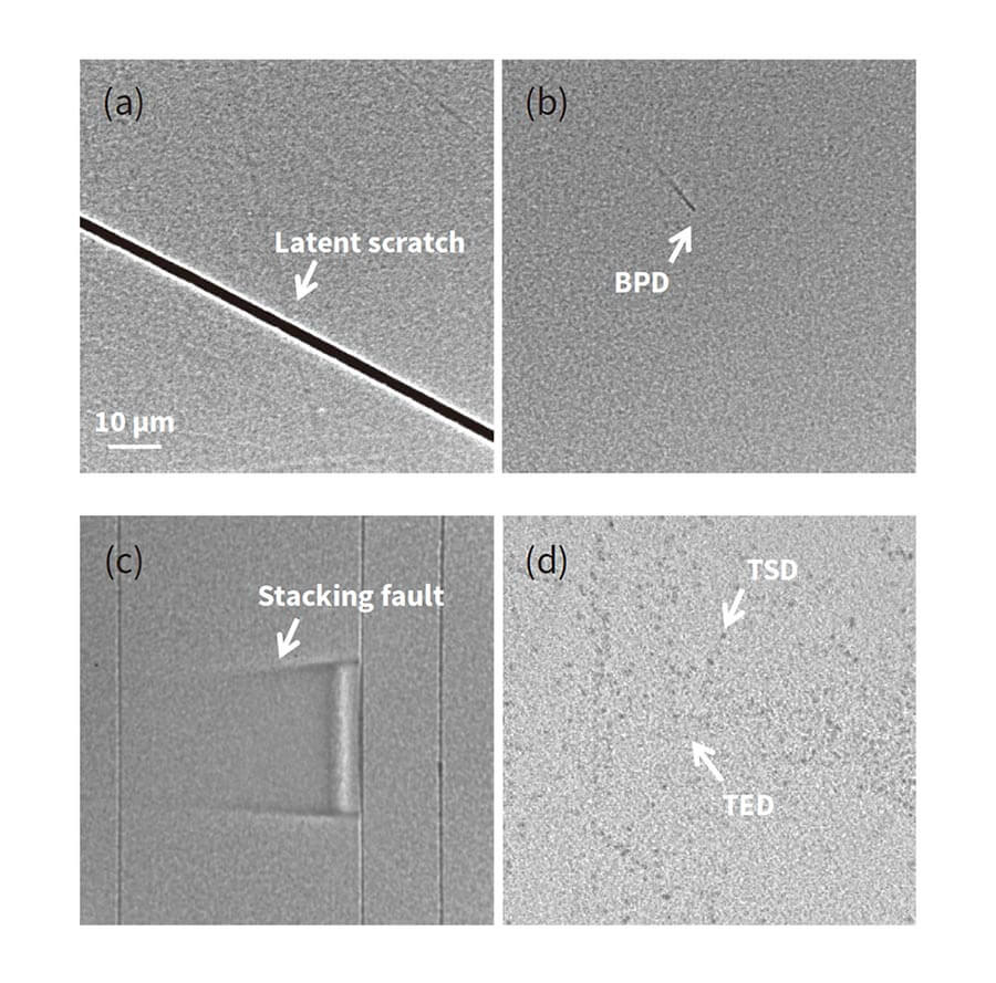 Photo (a) shows a bulk wafer latent scratch. Photo (b) shows a bulk wafer BPD. Photo (c) shows an epi wafer stacking fault. The straight vertical lines are level differences created by the overlapping of multiple atom layers (known as step bunching). Photo (d) shows epi wafer threading dislocations. Multiple dislocations have been detected. The dark spots are TSDs, and the light spots are TEDs. Typical examples are indicated by the arrows.
The Mirelis VM1000 mirror electron inspection system has a mirror electron microscope, a graphical user interface (GUI) to facilitate operations such as automatic wafer transport and automatic imaging recipe creation, and image processing software for automatic defect extraction (see Figure 4). It supports wafer sizes of 3, 4, and 6 inches, has an electron beam current of 1 to 2 nA, uses a charge-coupled device (CCD) camera for imaging, and photographs a single mirror electron image (80 μm squared) in 0.1 second (under standard conditions). It can provide automatic consecutive imaging to capture an image size of up to 2.5 mm squared per inspection location. The time required for imaging is 25 minutes when nine wafer locations are selected and each is captured at a size of 1 mm squared.
The number of images obtained by automatic imaging can be several thousand or more depending on how the imaging recipe is programmed, so the system comes with image processing software that extracts defects from large volumes of images. This software can inspect all the images using a user-specified image brightness threshold value and defect contrast magnitude (pixel value) threshold value, to identify inspection images containing defects and output a list of feature values related to defect positions and defect image brightness values and shapes.
Figure 4—Mirelis VM1000 Photo and Main Specifications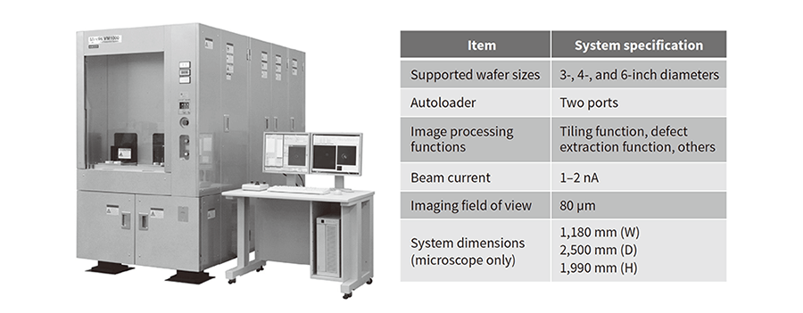 The name Mirelis is a portmanteau of “mirror electron inspection system.”
Figure 5—Manufacturer-specific Differences in Bulk Wafer Surface Quality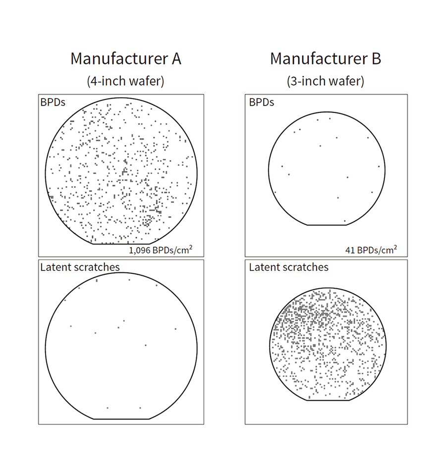 The imaging locations at which BPDs or latent scratches (processing damage) were detected in mirror electron images inspected by the Mirelis VM1000 at a pitch of about 0.8 mm are shown here as wafer maps. These wafer maps show that each manufacturer has characteristic crystal growth technology and polishing technology. Manufacturer A’s wafer has many BPDs and few latent scratches, while Manufacturer B’s wafer shows the opposite tendency.
Figure 5 shows the result of mapping distributions of BPDs and latent scratches (a typical type of processing damage) obtained by inspecting a commercially available 4-inch bulk wafer (Manufacturer A) and 3-inch bulk wafer (Manufacturer B) using the Mirelis VM1000. The numbers of BPDs per unit area (BPDs/cm2) are also shown. The imaging points are set to an interval of about 0.8 mm over the entire wafer surface, and the imaging locations at which latent scratches or BPDs are present in captured mirror electron images are marked. The imaging time was about 150 minutes for the 4-inch wafer and about 80 minutes for the 3-inch wafer. As shown, there is a large difference in quality between the manufacturers in terms of surface processing state (extent of latent scratches) and BPD density. Manufacturer A's wafer is seen to have few latent scratches and be largely unaffected by unevenness generated during epitaxial film formation. Devices manufactured from such wafers could be expected to generate few initial failures, but the high BPD density could result in conductivity deterioration in diodes. Manufacturer B's wafer is seen to have high crystal quality with low BPD density, but unevenness originating from latent scratches generated during epitaxial layer formation has been generated. Devices made from such wafers may generate many initial failures as a result. Epitaxial film formation for device manufacturing has previously been done without this quality information, so Mirelis VM1000 should be of great benefit to development work designed to improve yield or device manufacturing processes.
This article has presented some examples of SiC wafer defect detection using a new detection principle made possible by Hitachi's Mirelis VM1000 mirror electron inspection system. Validating the new method's effectiveness will require extensive time and creative input. To pursue the area of collaborative creation, Hitachi High-Technologies Corporation has engaged in joint research and collaborations with universities, research organizations, competitors, and clients. The company plans to continue its pursuit of collaborative creation as it works on creating attractive applications for inspection and measurement technologies in contribution to social innovation.
The development of the mirror electron inspection system described in this article was made possible by extensive assistance from Professor Toshiyuki Isshiki of the Kyoto Institute of Technology, along with members of Denso Corporation, the National Institute of Advanced Industrial Science and Technology, and the Central Research Institute of Electric Power Industry. The authors would like to express their heartfelt appreciation.
