World-leading Measuring Instruments and Systems
Hitachi FineSAT Series and ES Series of Scanning Acoustic Tomographs
To ensure the reliability of electronic parts, a growing number of industries are using nondestructive methods of high-resolution inspections and 100% inspections. Hitachi Power Solutions provides the FineSAT and ES series of scanning acoustic tomographs, and to meet demand for high-resolution inspections, it has developed a high-frequency, high-S/N ratio transducer with a nominal ultrasonic frequency of 400 MHz, and a wideband ultrasonic flaw detector. While conventional transducers (with a nominal frequency of 300 MHz) and flaw detectors can detect rectangular defects as small as 2.5 µm in width, the developed technologies can detect defects as small as 1 µm in width. To meet demand for 100% inspections of mass-produced items, the company has created a system that enables short takt-time scanning by combining the high scanning speed of the ES series with the ability to scan two interfaces simultaneously and image processing technology.


The rise of electric vehicles and increasingly advanced automotive electronic control is creating a growing demand for 100% inspections by nondestructive methods done to ensure the reliability of the electronic parts on which human lives depend. Increasingly compact high-performance mobile products are also creating demand for high-resolution nondestructive inspections. To respond to these market trends, Hitachi Power Solutions Co., Ltd. has developed and provides the FineSAT series of scanning acoustic tomographs and the ES series of high-speed electronic scanning acoustic tomographs (see Figure 1). FineSAT series models have a number of different scanning functions and are suited to both standard- and high-resolution measurement. ES series models support high-speed measurement and are used as the basic equipment units behind in-line inspection systems for vehicle-mounted power devices.
Figure 1—FineSAT Type V Scanning Acoustic Tomograph (Left) and ES5100 High-speed Electronic Scanning Acoustic Tomograph (Right)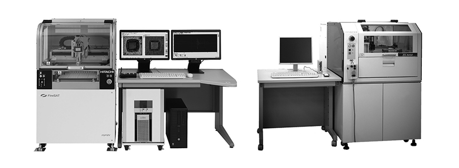 The FineSAT series has a number of different scanning functions and is suited to high-resolution measurement, while the ES series excels at high-speed measurement.
As shown in Figure 2, reflection and transmission take place at the layer interface when ultrasonic waves are emitted onto a specimen composed of Medium 1 and Medium 2 in layers. The reflected wave intensity (R) is given by:

where Z1 and Z2 are the acoustic impedance of Medium 1 and Medium 2, and I is the incident wave intensity.
The device used to oscillate the ultrasonic waves emitted onto the specimen and receive the reflected waves back from the specimen is called a transducer. Scanning acoustic tomographs provide planar measurement images of arbitrary depth within the specimen by scanning the transducer in the X-Y plane while providing a graduated display of the intensity of the reflected or transmitted wave for the ultrasonic wave received at each point. Intensities are displayed as grayscale shades.
Acoustic impedance is a measure of how easily sound propagates through a medium. It is highest for solids, lower for liquids, and lowest for gases. The acoustic impedance values of gases are at least 3 orders of magnitude lower than those of solids. Due to this large difference in acoustic impedance, nearly 100% of an incident wave is reflected by delaminations and voids. As a result, reflection method images provide a large contrast with the surroundings, enabling defect detection. For delaminations, detection is possible when the gap in the depth direction is 5 nm(1).
Figure 2—Principle of Ultrasonic Wave-based Defect Detection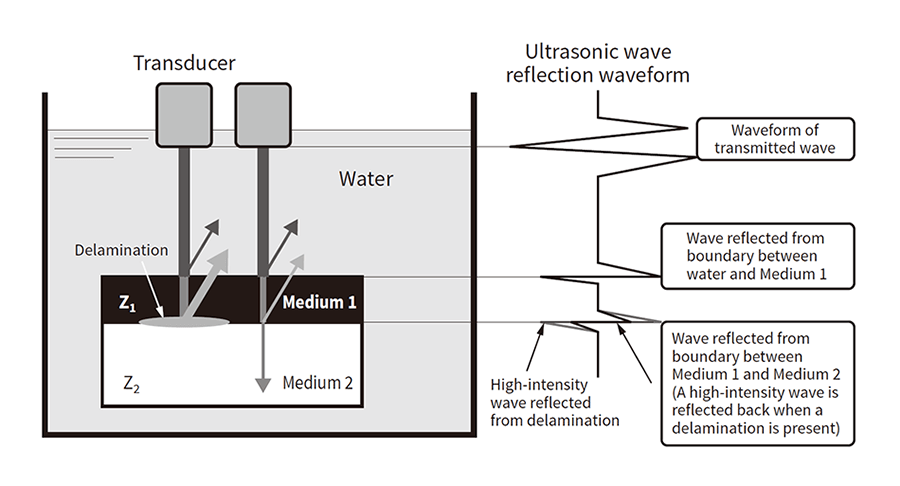 When ultrasonic waves are emitted onto a specimen, they are reflected from interfaces. When gas is present at an interface, a larger reflection wave intensity is obtained from that location than from others, enabling it to be detected as a defect.
FineSAT uses a single lens to focus an ultrasonic wave generated by a single oscillator, and emit it onto the specimen. An inspection image is obtained by using the transducer to mechanically scan the ultrasonic beam in the X-Y plane at a minute pitch.
In contrast, the ES5100 uses an electronic scanning method and the array transducer illustrated in Figure 3 to perform measurement. The array transducer has a large number of oscillators (up to 384 elements) arranged in strips. The oscillators in use are switched electronically in sequence (electronic scanning) to enable instantaneous imaging of a width of 30 mm in the Y direction. Phased array technology is used to vary the timing at which ultrasonic waves from multiple oscillators (up to 32 elements) are transmitted and received , enabling the depth of focus to be controlled in the Y direction.
Figure 3—Schematic Illustration of Array Transducer Electronic Scanning and High-speed Measurement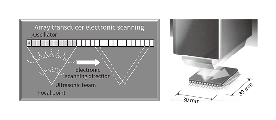 Instantaneous imaging of a width of 30 mm is made possible by sequentially switching the oscillators in use. The depth of focus can be controlled by adjusting the ultrasonic wave transmission/reception timing of multiple oscillators.
The increasing miniaturization of electronic devices is resulting in minute defects having major impacts on functionality, creating a growing demand for high-resolution inspections. Transducers for high-resolution measurement usually have an acoustic lens at the tip, and emit a focused beam onto the specimen. The spot size diameter d of a beam focused in water exhibits the correlation expressed by the formula below in terms of the focal distance F, acoustic lens aperture diameter D, and ultrasonic wave frequency f.

The ultrasonic beam diameter must be narrowed to improve resolution. As indicated by the formula above, it can be narrowed by decreasing the lens focal distance F, increasing the lens aperture diameter D, or increasing the ultrasonic wave frequency f. But the amount by which the focal distance F can be decreased is limited by the material and thickness of the specimen. Similarly, increasing the lens aperture diameter D generates total reflection of the ultrasonic beam emitted from the outer part of the lens in accordance with Snell's law, preventing the ultrasonic waves from penetrating into the specimen. Adjusting these two parameters will only improve resolution to a limited degree. So despite the problem of ultrasonic wave attenuation increasing within materials as the wave frequency increases, increasing the frequency is the most effective method for improving the resolution.
FineSAT series models use two new technologies developed by Hitachi Power Solutions: a high-frequency, high-sensitivity transducer (the A series transducer) and a new type of flaw detector that can output narrow pulses supporting high-frequency transmission. The new flaw detector lets FineSAT support the 400 MHz maximum nominal frequency of the new A series transducer, an improvement over the 300 MHz maximum nominal frequency of the conventional high-frequency transducer (the ZnO transducer).
Figure 4 shows the results of validation testing done to demonstrate the benefits of using the A series transducer and new flaw detector mentioned above. The specimen was created from a silicon (Si) wafer with a thickness of 550 μm and indentations 170 nm in depth formed on it as artificial defects. Another Si wafer 150 μm in thickness was bonded to the first wafer so as to envelop the area of the indentations within the material. The artificial defects were of two different shapes. One type were rectangles with a length of 2 mm and widths of from 1.0 to 300 μm. Figure 4 (a) shows the measurement results for this type. The other type were circles with diameters of from 1.0 to 128 μm. Figure 4 (b) shows the measurement results for this type.
The top images for each defect type are the measurement images obtained when using the conventional flaw detector with a ZnO transducer (12M2.0) of 300 MHz nominal frequency and 2.0 mm focal distance. The bottom images are the measurement images obtained when using the new flaw detector with a transducer (A16M2.0) of 400 MHz nominal frequency and 2.0 mm focal distance. The first setup was able to detect rectangular defects as small as 2.5 μm in width and circular defects as small as 8.0 μm in diameter. The second setup using the new technology was able to detect rectangular defects as small as 1.0 μm in width (the narrowest created) and circular defects as small as 4.0 μm in diameter. These findings demonstrate an improvement in defect detection ability.
Figure 5 shows an example of measurement of a commercially available large-scale integrated (LSI) circuit at higher resolution. Figure 5 (a) shows the measurement result when using the conventional flaw detector with a ZnO transducer (12M8.1) of 300 MHz nominal frequency and 8.1 mm focal distance. Figure 5 (b) shows the measurement result when using the new flaw detector with a transducer (A16M8.1) of 400 MHz nominal frequency and 8.1 mm focal distance. As shown by the intensity profiles between points A and B, there was a higher light/dark contrast for the new flaw detector used with the A series transducer than for the conventional flaw detector used with the ZnO transducer, and a more clearly visible internal structure.
Figure 4—Measurement Results for Artificial Defects in Bonded Wafer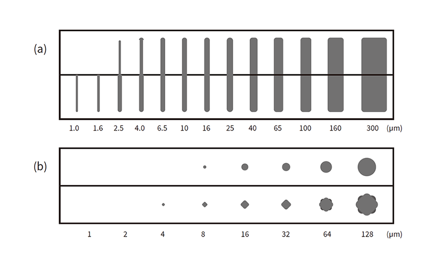 Illustration (a) shows the measurement results for rectangular defects. Illustration (b) shows the results for circular defects. The top parts of each illustration were obtained with a 300 MHz condition, and the bottom parts with a 400 MHz condition. The numbers at the bottom of each image are the artificial defect widths and diameters (μm).
Figure 5—Commercially Available LSI Measurement Images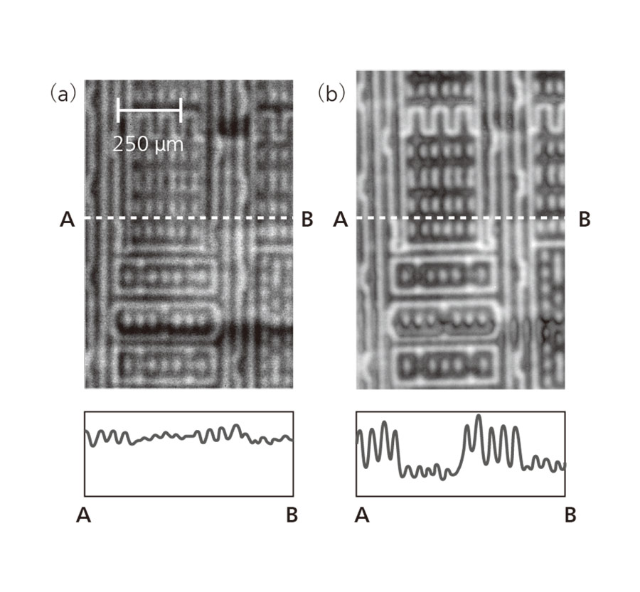 Photo (a) is the image obtained with a 300 MHz transducer. Photo (b) is the image obtained with a 400 MHz transducer. The graphs at the bottom are the cross-sectional ultrasonic wave profiles between Points A and B. As shown, a clearer light/dark contrast was obtained using the 400 MHz transducer.
As shown on the left side of Figure 6, the conventional ES5100 model performs planar imaging by focusing the ultrasonic wave on the interface for defect detection, and applying a gate to the waveform reflected back from the interface. So one measurement done by one array transducer only enables observation of one interface (single- transducer/single-gate measurement).
But in practice, situations in which only one interface needs to be observed are rare. Inspection images of multiple interfaces are needed, so Hitachi Power Solutions has developed technology with the ability to scan two interfaces simultaneously (single- transducer/dual-gate measurement). This technology focuses the ultrasonic wave near the midpoint of neighboring interfaces, applies a gate to the waveform reflected back from the two interfaces before and after the focal position in the direction of ultrasonic wave propagation, and inputs the result into a signal processor for pulse height analysis.
Since this method does not link the focal point to the interfaces that reflect the waveform back after gate application, the expectation was that it would miss defects due to drops in signal intensity. So the company conducted a validation test using a measurement condition typically used in power device measurement (0.2 mm pitch). As shown in Figure 7, it was found that despite image deterioration, detection itself was possible. So the method was combined with image processing technology to work on improving it and reducing missed defects.
Figure 6—Single-transducer/Dual-gate Measurement Illustration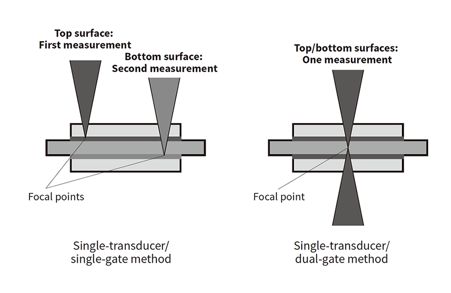 The single-transducer/single-gate method focuses on the interface to be measured, and captures the wave reflected back from that interface to form the image. The single-transducer/dual-gate method focuses between two neighboring interfaces, and forms the image by capturing the waves reflected back from both interfaces.
Figure 7—Captured Images and Image Quality Improvement Enabled by Scanning Two Interfaces Simultaneously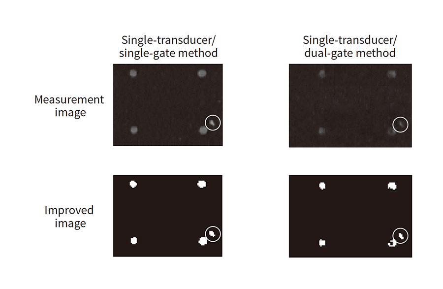 Drops in signal intensity were expected to lower the detection performance of the single-transducer/dual-gate method, but combining it with image sharpening technology has improved image quality and prevented missed defects.
This article has discussed high-speed and high-resolution detection technologies. High-speed defect detection technologies help improve the reliability of electronic parts, an increasingly important requirement amid the rise of electric vehicles and increasingly advanced automotive electronic control. High-resolution detection technologies support today's increasingly compact and higher-performance mobile products.
The FineSAT series uses the new A series transducer, with a 400 MHz nominal frequency, along with a new flaw detector supporting it. It has demonstrated its ability to detect rectangular defects with a width as small as 1 μm, and circular defects with a diameter as small as 4 μm. The ES series performs electronic scanning using an array transducer. It excels at high-speed defect detection, and further increases speed using technology that gives it the ability to scan two interfaces simultaneously. The trends toward electric vehicles and increasingly advanced automotive electronic control are expected to increase in the coming years. Hitachi Power Solutions is planning to address these needs by working on more advanced high-resolution and high-speed defect detection technologies.
