Along with the growing role of digital technology in people’s way of life, society also has a need to reduce power consumption to help achieve carbon neutrality. While leading semiconductor manufacturers are pushing ahead with device development in an effort to overcome these issues, many obstacles remain to achieve higher speeds, larger capacities, and lower power consumption. Through its semiconductor metrology and inspection business, Hitachi High-Tech Corporation is helping leading semiconductor manufacturers improve their production yields. This article describes a new metrology solution from Hitachi High-Tech that is intended to help improve the production yield for increasingly complex semiconductors as well as the future prospects for this technology.


Along with maintaining wellbeing and the standard of living while also addressing global-scale climate change, the modern world is being driven to make the transition to decarbonization, the circular economy, and decentralized societies(1). It is also no exaggeration to say that the digital technologies essential to achieving a circular economy are underpinned by improvements in semiconductor speed, capacity and power consumption. While semiconductor manufacturers are needing to take on increasingly complex manufacturing technologies in pursuit of new device designs, materials, and manufacturing processes, they are also facing problems with longer development times and yield loss.
The critical dimension scanning electron microscopes (CD-SEM) of Hitachi High-Tech Corporation have the role of measuring microelectronics pattern dimensions in device manufacturing and have become a de facto standard with the 5,600 instruments shipped to date representing a market share of more than 75%(2). Along with this comes ongoing demand for solutions capable of meeting new measurement requirements as semiconductors become more complex.
Advanced semiconductor devices are manufactured in high volumes by fabricating a large number of chips on 300-mm silicon wafers. Chip production involves a series of processes, including forming patterns on a 10-nm scale together with transistors, contacts, and interconnects(3). After fabrication, the wafer is diced into individual chips that are subject to a final inspection before those that pass are dispatched. The number of process steps has been increasing node by node and the manufacturing lead time required before shipping can take more than six months. Unfortunately, a variety of different defects can arise across these manufacturing processes that result in defective chips being discarded. This makes yield improvement an important business issue in the semiconductor industry where economies of scale are achieved through high-volume manufacturing.
Hitachi High-Tech’s CD-SEMs assist with yield improvement by measuring the dimensions of semiconductor circuit patterns. The instruments can measure dimensional or positioning errors by scanning an electron beam over the circuit pattern to obtain an electron microscope image of the surface(4). Of particular importance is to be able to perform in-line measurement to obtain parameters such as critical dimensions that characterize process quality without interrupting the production process. By monitoring variations in critical dimensions, it is possible to control processes before they cause yield loss.
These capabilities provided by CD-SEMs have played a major role in semiconductor miniaturization since the 1980s. This is because measuring the planar dimensions of a semiconductor is equivalent to measuring its performance(4). With the shift to three-dimensional (3D) semiconductor designs since 2010(5), however, the requirements have expanded to include 3D metrology (the measurement of 3D shape) as well as planar dimensions(6). Semiconductors are also expected to become increasingly complex in the future. This is creating a need for a wide range of other measurement data, not just pattern dimensions.
This section describes two solutions for these new measurement requirements: for 3D metrology and for electrical property measurement respectively.
Figure 1 — 3D Metrology for Semiconductors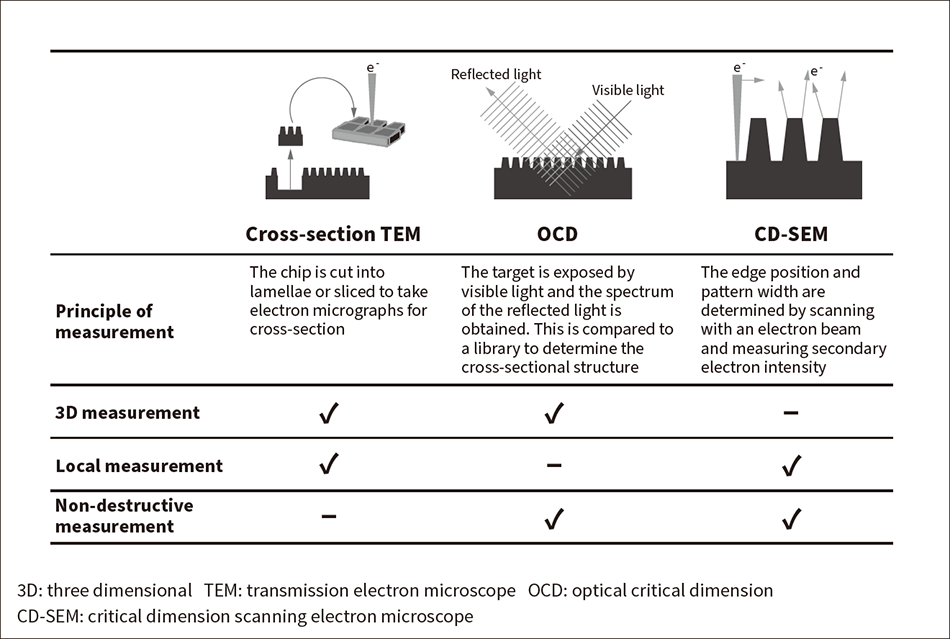 No single measurement technique satisfies all three requirements of in-line 3D metrology (3D measurement, local measurement, and non-destructive measurement). 3D measurement of a CD-SEM is an important technology for achieving all three at the same time.
Figure 1 shows how 3D shape measurement is performed for semiconductor devices(7). The most commonly used method at present is to slice the device and use a transmission electron microscope (TEM) to observe its cross-section directly. While this technique is widely used in failure analysis or in process optimization during development, being a destructive technique means it cannot be used for in-line measurement. Instead, it is a technique called optical critical dimension (OCD) spectroscopy that is mainly used for in-line metrology(7). A beam of visible light irradiates the chip and the change in the spectrum of the reflected light is used to determine the shape of the circuit pattern in the illuminated area. While this technique is non-destructive and able to determine 3D shapes with high speed, its drawback is that it can only provide the averaged shape across the region of the illuminated spot (about 10 µm). The problem with this is that the control of semiconductor pattern yield has a strong need for more localized measurement to enable monitoring for disruptions in the shape of individual circuit patterns. CD-SEMs, in contrast, although capable of both local and non-destructive measurement, have traditionally been designed for the measurement of lateral dimensions, meaning they are not well suited to acquiring 3D shape information(6).
This led Hitachi High-Tech to set about developing a 3D metrology solution that could take advantage of the local and non-destructive measurement capabilities of CD-SEMs (see Figure 2). Conventionally, CD-SEMs have been used to measure lateral dimensions, determining the positions of circuit pattern sidewalls by detecting the secondary electron enhanced at sidewalls. The new metrology technique uses backscattered electrons from the bottom of trenches. As these backscattered electrons take a straight trajectory, the number of escaped electrons depends on the pattern depth. That is, changes in the depth of the semiconductor pattern change the angle of the opening at the top of the trench relative to the bottom. Therefore, the depth can be estimated by measuring the quantity of backscattered electrons and the width of this opening(8).
To give an example of how this can be used to monitor pattern depth, Figure 3 (a) shows a CD-SEM image of such a trench. The black vertical bands represent the bottoms of trenches. Figure 3 (b) shows a greyscale image that presents the results of non-destructive local measurement of the 102 chips on a wafer performed utilizing the principle illustrated in Figure 2, where darker grey indicates greater trench depth. The results show a lack of uniformity in trench depth across the wafer, with a concentric distribution of depths that are deepest in the central region. The depth variability across the wafer in this case was 8%. This result was also found to be in agreement with the SEM cross-section shown in Figure 3 (c). In other words, this technique helps chip makers to improve production yield by providing depth distribution information obtained in the production process without cleaving wafers.
Figure 2 — Comparison of Conventional CD-SEM and New 3D Metrology Technique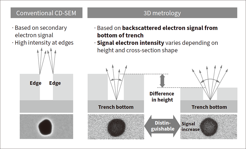 The secondary electron signal is useful for determining edge positions because its intensity increases at edges. The backscattered electron signal from the bottom of the trench, meanwhile, depends on the angle of the opening at the top and this allows the pattern depth to be estimated.
Figure 3 — Example Measurement of Trench Pattern Depth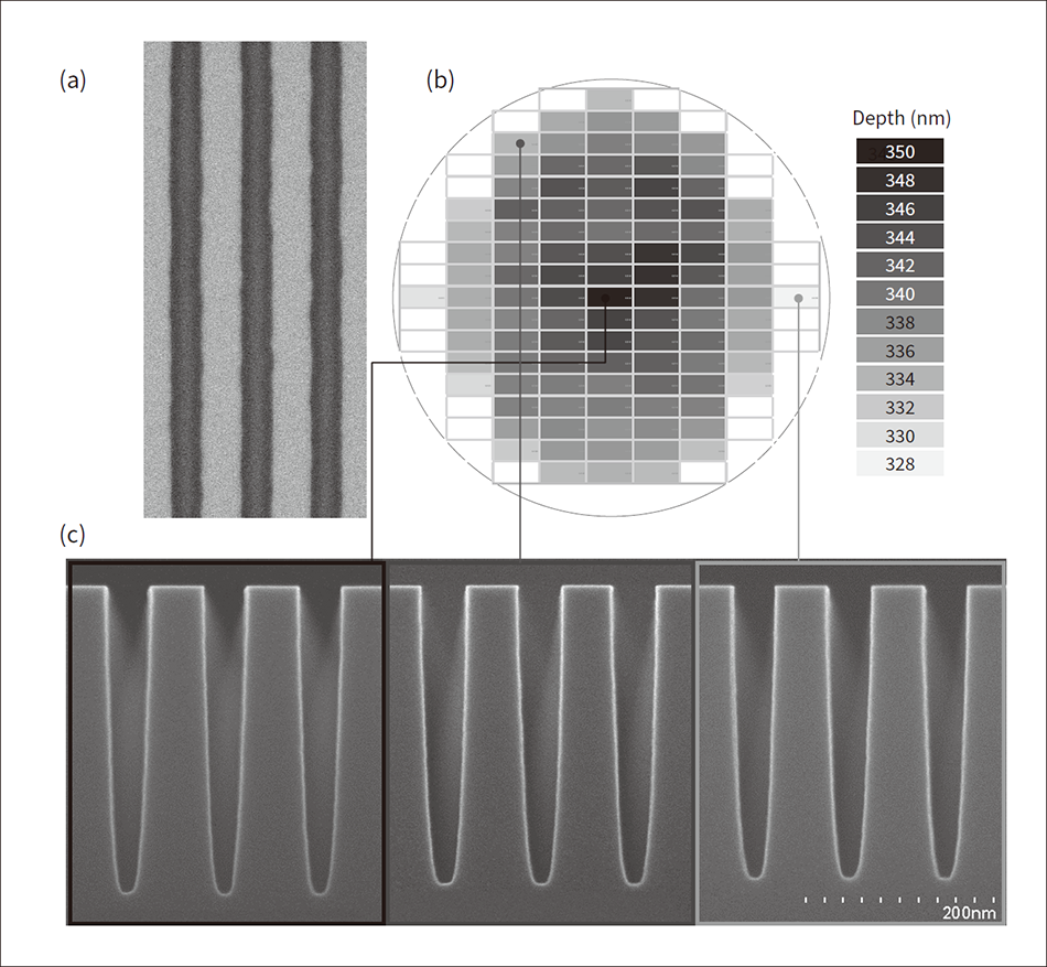 Figure (a) is an SEM image obtained using backscattered electrons. The dark vertical bands represent trenches, showing the intensity of the signal from the bottom of the trenches. The image in (b) is a greyscale map of the trench depth distribution on the upper surface of a wafer, with darker color indicating greater depth. The image in (c) shows the cross-section of a trench.
As semiconductors become more complex, it becomes increasingly difficult to assess their performance by dimensions and shape alone. Impurities and film defects, for example, can also cause semiconductors to perform abnormally. The early detection of such device defects requires electrical property measurement by directly probing the device working voltage.
Figure 4 shows how electrical property measurements are performed. One such commonly used method is the probe test shown in Figure 4 (a). This uses a probe to apply a voltage to the device and measures the resulting response(9). The problem is that attaching a probe to the circuit requires the forming of a large probe pad after the circuit element fabrication and subsequent interconnect process (which takes several months) have been completed. However, Hitachi High-Tech has recognized that being able to perform electrical property measurement at an earlier stage would help to shorten customers’ development cycle times. Probes that have been miniaturized to enable earlier measurement are called nanoprobes(10) and these nanometer-scale probes can be manipulated in the field of view of an SEM to make contact with individual chip transistors [see Figure 4 (b)]. Their use enables the measurement of semiconductor properties without having to wait for the interconnect process to be completed. The challenge, however, is how to identify the correct transistor to measure. As the number of transistors continues to increase in accordance with Moore’s Law, logic bit densities can now be as high as 40 million per mm2 or more(11). Finding the right transistors to measure out of this huge number requires a system for rapidly identifying electrical abnormalities over a wide area. Non-contact measurement using an electron beam is one way of finding changes in electrical properties through the rapid acquisition of wide-area images and it can be used in tandem with the nanoprobe technique described above to provide a solution for the early measurement of electrical properties [see Figure 4 (c)].
A simple way to explain how an electron beam can be used to measure electrical properties(12) (see Figure 5) is as follows. The speed at which electrons propagate through a specimen when it is scanned by an electron beam is determined by the charging and discharging characteristics of the circuit formed by the associated electrical resistance and capacitance. This means that the surface potential of the specimen will also change over time by the same mechanism. As the level of the secondary electron signal varies depending on the surface potential, the changes in this signal over time can be used to measure this potential. From this, the resistance and capacitance in the scanned area can be determined. Hitachi High-Tech has utilized this principle for non-contact electrical property measurement to develop a variable-time (VT) scan technique that increases the SEM image contrast based on electron relaxation(13), (14).
Figure 4 — Measurement of Electrical Properties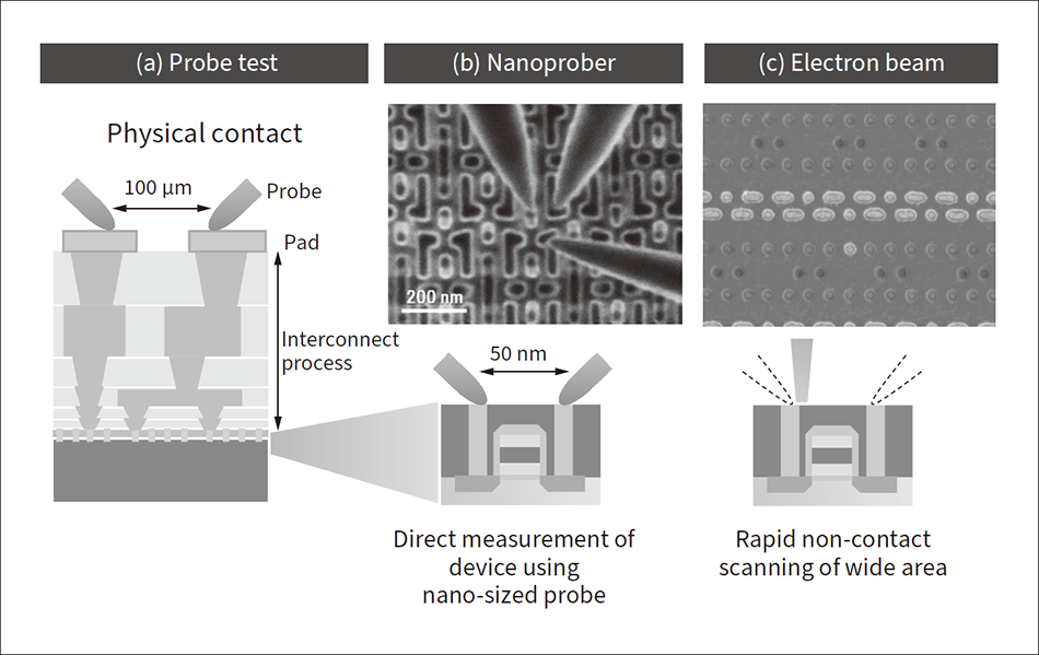 Probe test, as shown in (a), is the most widely used method for measuring electrical properties. Because this method needs a large probe contact pad and so has to wait until after the interconnect process, it can only be performed in the back-end-of-line stage of semiconductor manufacturing. The nanoprobe technique shown in (b), on the other hand, can perform direct measurements on transistors using a miniaturized probe. This technique is mainly used for fault analysis after first identifying which transistor to measure. The electron beam technique in (c), meanwhile, can perform non-contact scanning of a wide area and so is used to identify defects.
Figure 5 — Principle of Electrical Property Measurement Using SEM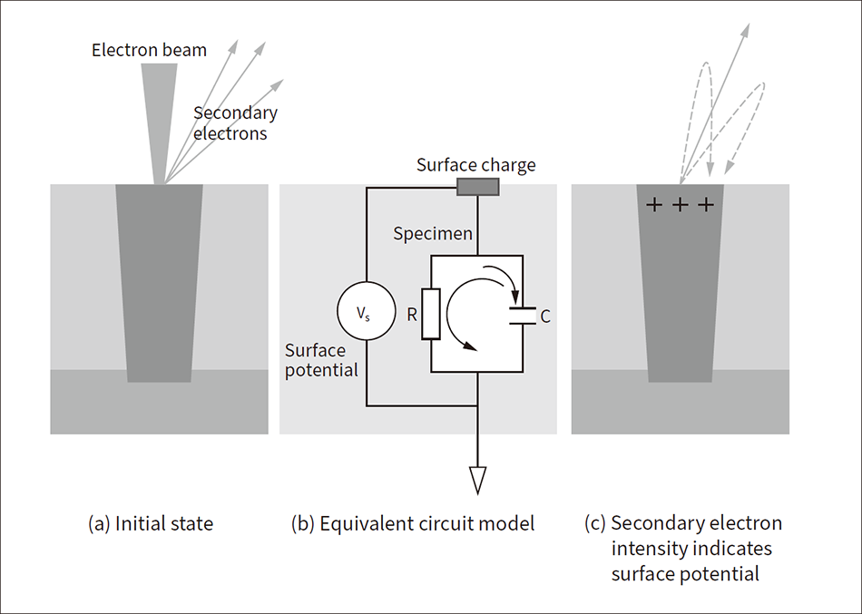 Considering the equivalent circuit formed by the resistance (R) and capacitance (C) of the specimen, the specimen’s surface charge can be determined from the relaxation of electron charge. As some of the emitted signal electrons will be attracted back to the specimen when the charge becomes positive, it is possible to determine the change in charge (voltage) from the change in the number of signal electrons. Using this principle, the resistance and capacitance values in the equivalent circuit can be estimated from the level of the secondary electron signal.
Figure 6 (a) shows an example of detecting a conduction defects in junctions. This involves a conventional source-drain junction for a field-effect transistor (FET) in which a p-n junction is sandwiched between the contact plug and substrate. Electrons from the plug cannot flow across the p-n junction formed by the n-type semiconductor of the junction and the p-type silicon (Si) substrate below it. Even if an open defect has been formed in the contact hole etching process, there is no way of distinguishing this as it makes no difference to how much electron flow is impeded. However, if a measurement technique such as VT scan is used that also responds to capacitance, this can induce a difference in how the level of charge changes over time. Figure 6 (b) shows a comparison of a conventional SEM image and one obtained using VT scan. The latter image shows a clear difference in the signal level for the defective plug.
Figure 6 — Detection of Open Defect Using VT Scan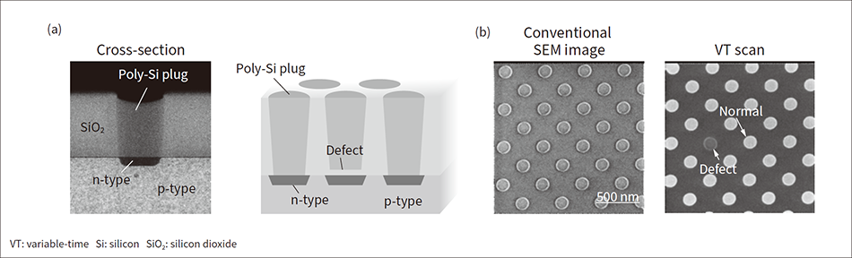 The figure shows how detection is performed on a semiconductor device in which a p-n junction is formed under a poly-Si plug. Because the transportation of electrons from the n-type to the p-type Si is blocked, the extent to which electron flow is impeded is the same regardless of whether a defect (open) is present or not, and therefore the defect cannot be detected by a conventional SEM image. With VT scan, on the other hand, charge transport is controlled by the resistance and capacitance of the equivalent circuit, thereby a defect can be visualized.
Figure 7 — Integrated Data Solution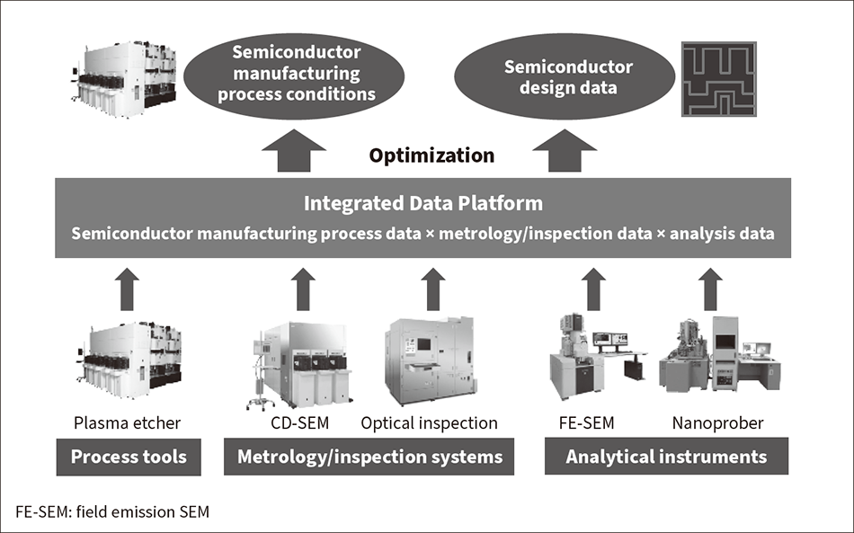 Manufacturing process conditions and design data can be optimized on the integrated data platform by collecting and analyzing data output from production equipment, metrology and inspection systems, and analytical instruments.
Steady advances are being made in the structures and materials of semiconductor devices. With more advanced devices, identifying the causes of yield loss can take a long time when restricted to only those measurement techniques and data in current use. On the other hand, yield improvement can be achieved quickly if one can combine metrology and inspection data from a variety of different instruments.
In addition to metrology and inspection systems such as the CD-SEM described in the preceding chapter that are used in the front-end-of-line stage of semiconductor production, Hitachi High-Tech also offers a range of equipment that includes plasma etchers for semiconductor device fabrication, nanoprobes for electrical property analysis, and field-emission SEMs (FE-SEMs) for observing devices in cross-section. By consolidating the various data output by these instruments on an integrated platform, including semiconductor device processing conditions, measurements, inspection data, and analysis data, it becomes possible to identify the different factors that influence yield loss (see Figure 7).
Semiconductor manufacturing uses a wide range of production equipment and design data. Accordingly, Hitachi High-Tech intends to contribute to semiconductor development and yield improvement by offering a wider range of data solutions in the future that integrate not only with its own products but also the customer’s production equipment, process data, and systems supplied by other vendors.
This article has presented examples of new performance evaluation techniques for the upstream stages of semiconductor manufacturing.
Alongside the ongoing advances in semiconductor devices, Hitachi High-Tech is contributing to social innovation by combining digital technologies that maximize the value of measurement data with its core electron beam technology to resolve the many challenges facing the increasingly complex tasks of semiconductor development and manufacturing.
