16 February 2022

Wei Sun
Research & Development Group, Hitachi, Ltd.
The growing need for 5G connectivity, Internet of Things (IoT), and big data is driving new growth in the semiconductor industry as the capability to store and process more data requires a large number of low-cost, high-performance semiconductor devices. Advanced semiconductor devices have moved from simple planar structures to complex three-dimensional (3D) structures, and one of the biggest developments is the 3D NAND memory.
To decrease the cost-per-bit, 3D-NAND manufacturers continue to increase the aspect ratio of channel holes. But it has become more difficult to etch the high-aspect-ratio (HAR) holes straightly as the etching process may cause defects like tilting, bowing, and twisting (see Figure 1) which will affect the device performance and the wafer yield. Therefore, metrology techniques are also required to be 3D to measure the geometry of the HAR hole.
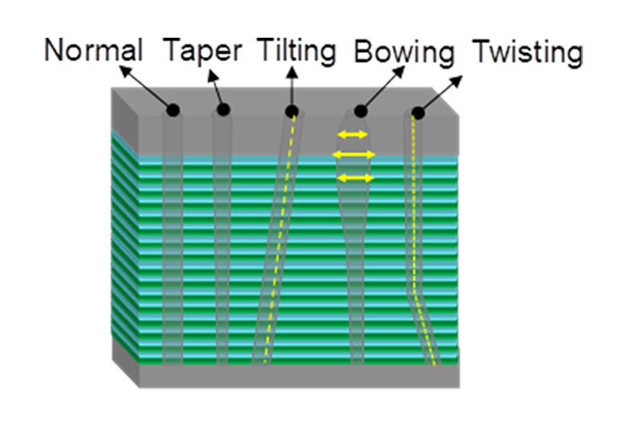
Figure 1. Various possible geometries of HAR holes after the etching process
Critical dimension scanning electron microscopy (CD-SEM), specialized to measure 2D pattern size from grey level SEM images, plays an important role in process control of semiconductor devices. Information on the third-dimension, however, is also embedded in the SEM image and can be explored from the signal intensity if the physical interaction between the electrons and the pattern is understood. This is effective when the 3D dimension of the pattern and its CD-SEM image data are available and consistent, but it does not always make sense in the semiconductor industry because the 3D dimension of the pattern is not always available for us to clarify the physical interaction. Our solution to this issue is using a combination of physical modeling to deep learning (DL).
To construct a DL model which outputs a 3D profile of HAR holes using the top-view SEM image as input data, a large number of training datasets are needed to learn the relationship. We created a physical model to represent the interaction between the electrons and the HAR hole using Monte Carlo simulation results so that the SEM signal intensities of the HAR hole having various geometries can be quickly calculated according to the physical formula (see Figure 2).
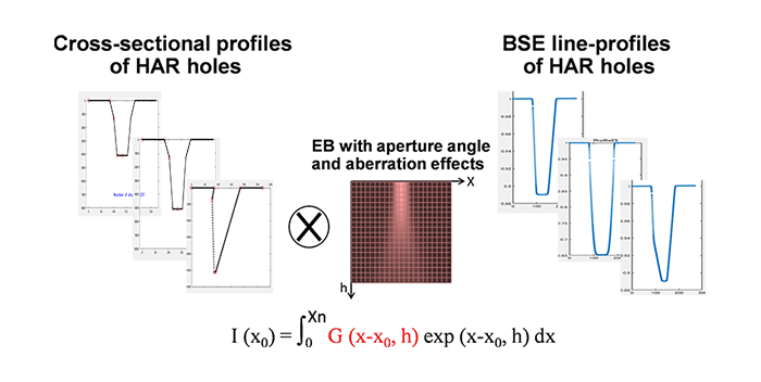
Figure 2. Numerical calculation of the dataset for deep learning according to the created physical formula
We also added some optical parameters related to the electron beam G(x,h) in the SEM tool to the physical model to improve the prediction accuracy. Using these datasets, we were able to create a convolutional neural network to predict the 3D profile of HAR hole. Experimental evaluations were performed with the trained DL model. The HAR holes with different profiles were etched in multiple silicon wafers through tuning the etching process and their geometries were measured from cross-section SEM images. We evaluated the prediction performance of the DL model by comparing the prediction with the cross-section SEM measurement (see Figure 3). The results showed that the DL model allowed us to predict the taper and bowing profile with good sensitivity and accuracy.
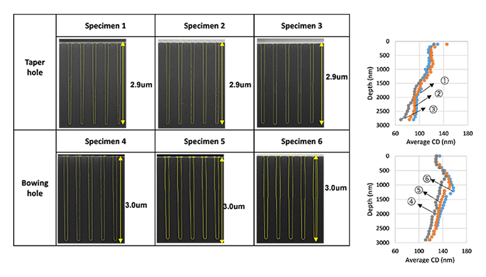
Figure 3. Cross-section SEM images of the HAR holes having different profiles and the prediction results obtained by the DL model
Accurate, stable, and reliable measurement performance is a given requirement in metrology and many technologies are still being developed to enable in-line 3D metrology for HAR features. While there are many challenges that need to be overcome before the DL approach can be used for process control in manufacturing, we believe that a solution combining physical modeling and deep learning is effective in addressing other issues in advanced metrology.
Details of this work can be found in our paper presented at SPIE Advanced Lithography 2021 [1].
