Advances in the power devices, motors, batteries, and control techniques used in electric rolling stock and other mobility applications are being utilized to improve system efficiency and achieve smaller size and higher reliability. This article describes two devices from Hitachi Power Semiconductor Device, Ltd. that offer high added-value. The first is a low-loss Si-IGBT module with more than 20 times the power cycling lifetime of previous modules and the other is a SiC MOSFET module with switching losses that are less than two-thirds those of previous products provided by Hitachi Power Semiconductor Device. Hitachi has estimated the value added when these devices are used in equipment applications and compared them to devices supplied in the past. When these two newly developed devices were used to build an active-neutral-point-clamp circuit, it delivered a 140% improvement in inverter output compared to previous devices from Hitachi Power Semiconductor Device.

Hitachi Power Semiconductor Device, Ltd. has long worked to enhance the price-performance of equipment through the supply of power devices. There are three steps in this process. The first step is to define the value added in terms of the maximum output current at which the semiconductor temperature (Tj) reaches the absolute maximum rated temperature.
The second step is to consider the mission profile for the equipment in which the power device is to be used and to define the expected lifetime based on the maximum output current that will occur during operation. In the case of mobility systems, which are subject to rapid output fluctuation, the maximum output current is determined from the power cycling lifetime for the module’s bonding and areas in contact with the heat sink. This maximum current is in many cases lower than the output current determined in the first step.
In the third step, the added value of the device is defined as the price-performance calculated by dividing the output power by the up-front cost subtracted by the difference in electricity running costs and battery cost (1). As energy costs have risen in recent years due to international conflicts and renewable energy surcharges, the benefits of reducing electricity running costs have grown in importance. By incorporating detailed information about the application with the help of the customer, this analysis can calculate the price-performance, which is to say, the benefit to the customer or added value precisely.
This article describes two power devices from Hitachi Power Semiconductor Device (HPSD) that offer high added value.
The first of these high-added-value power devices is a silicon insulated gate bipolar transistor (Si-IGBT) module with a power cycling lifetime more than 20 times the previous modules. The other is a silicon carbide metal-oxide-semiconductor field-effect transistor (SiC MOSFET) module with switching losses that are less than two-thirds those of previous modules. With reference to the equipment in which the power devices are to be used, the added value is calculated in accordance with the first step above and compared with that of previous products.
By taking maximum advantage of the high speed and low switching losses of SiC, HPSD’s “next high power density dual” (nHPD2)(2) power devices reduce drive circuit inductance and cumulative current rating to 20% that of previous models. The low inductance increases the maximum power that can be handled by minimizing the voltage spikes that result from rapid switching. HPSD has been looking at how to use the package to achieve low losses, high thermal dissipation, long device lifetime, and enhanced functionality in Si as well as SiC devices.
The Roll2Rail project has defined specifications for the power devices that railway system vendors will require in the future(3). This requires a 20-fold improvement over previous devices in power cycling lifetime, to one million cycles at Tj,max = 175°C and ΔTj = 100 K(4). Unfortunately, this is difficult to achieve with conventional bonding using solder and aluminum (Al) wire. Recognizing that a longer power cycling lifetime provides a quantitative boost to system value, HPSD has been working to improve this parameter(5). In the latest generation of semiconductor chips, power cycling lifetime has been considerably enhanced by using sintered copper on the bottom surface of the chip and high-strength materials for the electrodes and wires on the top side (see Figure 1).
Figure 2 shows the results of device testing. At more than 1.5 million cycles, the power cycling lifetime is more than 20 times longer than previous modules that used conventional solder and Al wire [see Figure 2 (a)], thereby satisfying the one-million-cycle lifetime requirement of Roll2Rail. Using the formula for power cycling lifetime, a lifetime prediction simulation was also performed based on the mission profile of 1,500-VDC/two-level metro rolling stock [see Figure 2 (b)]. The maximum output current for a 30-year expected life has been increased by 180% compared to a module with conventional solder and Al wire [see Figure 2 (c)]. Samples of the module are currently available (part no.: MBM800GS33G2).
Figure 1 — Diagrams of Devices with Enhanced Power Cycle Performance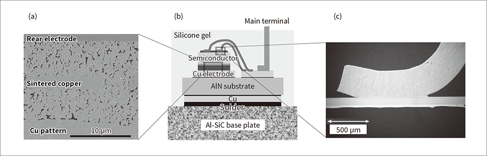 Image (a) was taken by a scanning electron microscope and shows the sintered copper layer under a chip, diagram (b) shows the module cross-section, and image (c) is the cross-section of a high-strength electrode and wire bonding.
Figure 2 — Verification of Power Cycling Lifetime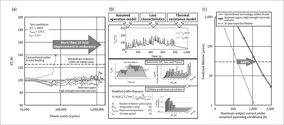 Graph (a) shows the trend in ΔTj over the course of power cycle testing, (b) shows the sequence of steps for calculating the lifetime for a given mission profile, and (c) shows the relationship between predicted lifetime and maximum current.
Being unipolar devices, SiC MOSFETs are capable of faster switching than Si-IGBTs and they significantly reduce switching losses(6). When higher output currents are needed, chips, sub-modules, and modules are connected in parallel. However, instability in this parallel system configuration can induce high-frequency oscillations of between several tens and a hundred MHz in the high-speed switching waveform(7). The nHPD2 modules have two device pairs and use the internal gate resistance [Rg(int)] to suppress this waveform noise (see Figure 3). Increasing the ratio of feedback to output capacitance and reducing the inductance across the source potentials help maintain system stability. This enables Rg(int) to be reduced while still suppressing high-frequency oscillations, reducing switching losses to 65% of those of previous modules (see Figure 4).
Figure 3 — Equivalent Circuit of Low-loss/High-capacity SiC MOSFET-nHPD2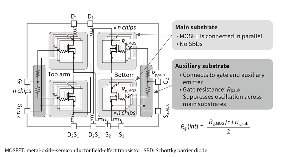 The circuit reduces the value of the Rg(int) resistance while also increasing the ratio of feedback to output capacitance and reducing the inductance across the source potentials to suppress high-frequency oscillations.
Figure 4 — Comparison of Switching Waveforms for Low-loss/High-capacity SiC MOSFET-nHPD2 and conventional SiC MOSFET Module and conventional SiC MOSFET Module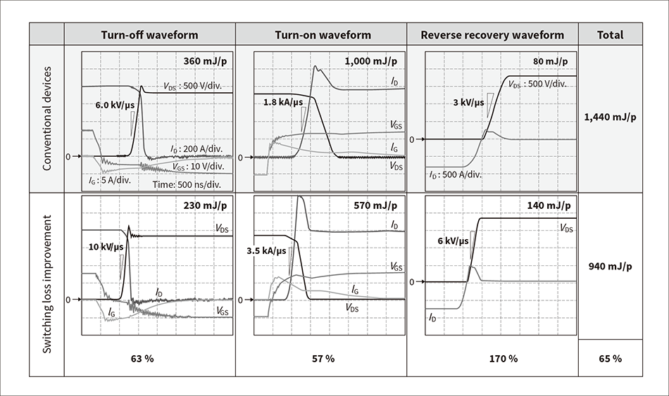 Switching losses are reduced to 65% of previous devices by reducing Rg(int) while also suppressing high-frequency oscillations.
An active-neutral-point-clamped (ANPC) inverter is one example of a system that can combine the two power devices. The dependence of maximum output current on carrier wave frequency was studied for such a system.
ANPC allows for the switching frequencies of direct-current (DC) and alternating-current (AC) devices to be set independently(8). The SiC MOSFET is used on the DC side where it can be mounted close to the DC capacitor to reduce inductance and the Si-IGBT is used on the AC load side where inductance is high. Output is maximized by using an approximate three-to-one ratio for the SiC MOSFET and Si-IGBT switching frequencies.
This was compared with a neutral-point-clamped (NPC) inverter using either 6.5-kV Si-IGBTs(9), innovative Si-IGBTs (i-Si-IGBTs)(10), or 3.3-kV SiC MOSFETs and Schottky barrier diodes (SBDs), and also with an ANPC inverter using conventional 3.3-kV Si-IGBTs and SiC MOSFETs. These are shown in columns (a) to (d), respectively, in Figure 5. The output current at which the bonding temperature is 15 K below the maximum rated temperature was then determined for an inverter DC voltage of 3.6 kVDC. It was also assumed that the coolant was at a temperature of 50°C and that its thermal resistance is inversely proportional to the device footprint area.
For a carrier wave in the 500-Hz-and-under range, the two-level inverter with 6.5-kV i-Si-IGBTs had the highest output. This configuration achieved more than double the output of the 6.5-kV Si-IGBTs used previously. At higher carrier frequencies, however, it was the ANPC inverter using the new power devices that had the highest output. When compared to the other ANPC inverter, the output for a 2-kHz carrier wave was 140% higher than when using the previous power devices (see Figure 6).
Figure 5 — Comparison of Circuit Topologies and Devices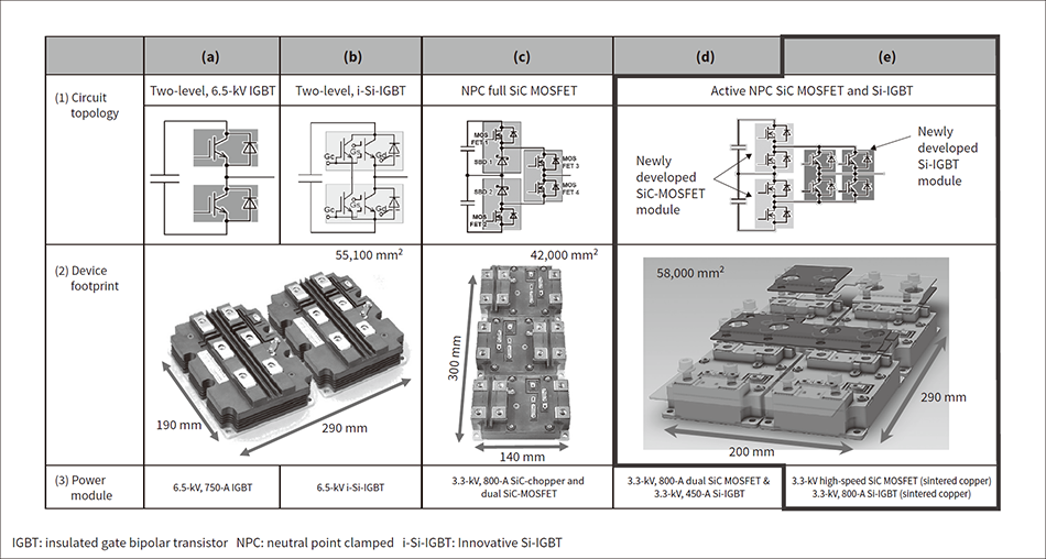 The diagram shows the inverter outputs for: (a) 6.5-kV Si-IGBT(9) two-level, (b) 6.5-kV i-Si-IGBT(10) two-level, (c) 3.3-kV SiC MOSFET and SBD NPC, (d) 3.3-kV Si-IGBT and SiC MOSFET ANPC, and (e) New 3.3-kV Si-IGBT and SiC MOSFET ANPC configurations.
Figure 6 — Comparison of Carrier Wave Frequency Dependance of Maximum Output Current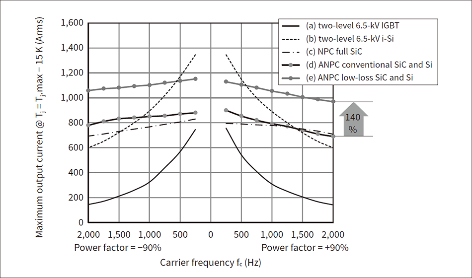 A two-level i-Si inverter has the highest output in the low frequency range and an ANPC inverter that combines the newly developed SiC module and highly reliable Si-IGBT module has the highest output in the high frequency range.
This article has compared the maximum output currents for the new power devices and their predecessors for a variety of circuit topographies. The next step is to consult with customers and calculate the maximum outputs at which the expected lifetime can be achieved for specific mission profiles. The added value over the device lifetime cycle is also determined by offsetting the difference in installation cost (including that of peripheral equipment) and the electricity running costs over a given time period against the device cost. HPSD also plans to identify the maximum cost-performance under different system operating conditions so as to offer the devices that best suit the needs of each customer.
