Contributing to image quality and clearer observation of changing objects
September 7, 2018
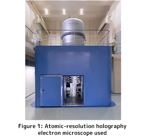
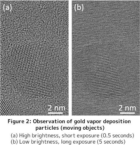
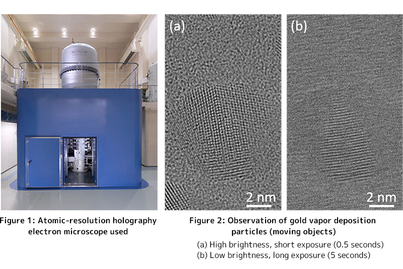
Hitachi, Ltd. today announced that it has achieved the world’s highest recorded brightness of 3×10¹⁴ A/m2sr with the atomic-resolution holography electron microscope*1 (Figure 1). This record-breaking achievement was attained by developing an electron-beam illumination system that stably emits electron beams with a high level of directivity over a sustained period of time, and by inventing a new improved method for measuring brightness – an important indicator of electron microscope performance. This achievement will improve image quality and allow for even clearer observations of moving or changing objects (Figure 2), as well as contribute to speed and sensitivity improvements in electron microscope imaging overall.
Image quality in electron microscopes become clearer with brighter electron beams just it improves in optical microscopes when the target of observation is exposed to higher levels of light. The luminosity of the electron beam is called brightness, and brightness is determined by the quantity and directivity (direction alignment) of electrons.
Hitachi has been developing holography electron microscopes*2 since 1966 as a tool to directly observe micro-region electromagnetic fields necessary for the development of next-generation highly functional material that will support future innovations in energy and resource conservation. Moreover, to clarify the mechanisms at work, atomic-level resolution is necessary. In February 2015, Hitachi announced the development of an atomic-resolution holography electron microscope with a point resolution of 43 picometers*3 under the "Funding Program for World-Leading Innovative R&D on Science and Technology" (FIRST Program). Since then Hitachi has continued efforts to improve measurement techniques and the performance of the atomic-resolution holography electron microscope.
The research results announced this time will be presented at the 19th International Microscopy Congress to be held from 9th to 14th September in Sydney, Australia.*4
External noise is known to affect the voltage fed into the accelerator electrodes which accelerate the extracted electrons, and the signals added to deflection coils which control direction. The external noise was thoroughly suppressed using electromagnetic shields and filter know-how to confine the dispersion in electron directivity. This resulted in an electron beam with a high directivity and extremely small dispersion (illumination semi-angle) of 4.0×10⁻⁹ rad. This number indicates that even if an electron beam traveled 250 km, it would only become blurred by about 2 mm horizontally.
A dedicated digital camera for electron microscopes*5 was used to measure the current distribution of electron beams with high accuracy. Noting that the relationship between directivity and the wave nature of electrons, a method was devised to calculate the directivity by quantitively measuring the wave nature of electron beam. The length of the region where interference fringes formed by the electron scattered by an aperture appeared, were measured to quantify the wave nature of the electron beam. Both measurements were combined to attain the brightness value.
When making observations at the atomic level, it is difficult to bring objects to a complete standstill for prolonged periods. However, the period of time used to take images (exposure time) can be shortened when brightness is improved as many electrons can be illuminated in a short period of time. As the exposure time is shortened, it is easier to acquire clearer images which appear to be at a complete standstill even if the objects are moving (Figure 2). For example, it is thought that this will display its influence in operando measurements where moving electron devices and reacting catalysts are observed directly through electron microscopes.
One wave property of electrons is that as brightness increases, it can be observed in a wider region and at a higher level of contrast. Thus the distribution of both weak and atomic-sized electric and magnetic fields can be captured. In addition, it allows for basic research in quantum physics to obtain a deeper elucidation of the wave-particle duality of electrons. For example, the collaborative research achievement announced in January 2018*6 by RIKEN, Osaka Prefecture University and Hitachi, used this technology.
Hitachi will use these results to continue the development of new materials to support a sustainable society, as well as continue to contribute to scientific development through collaborative research with external organizations such as research institutes and the Atomic Scale Electromagnetic Field Analysis Platform,*7 a part of the Ministry of Education, Culture, Sports, Science and Technology’s project to promote the sharing of cutting-edge research infrastructure.*8
The quality of an electron microscope image is determined by resolution and the signal to noise ratio (SN ratio). Resolution is determined by the properties of electron microscope lenses and the luminosity of the electron beams that illuminate the target. SN ratio, on the other hand, is determined by the luminosity of electron beams and the properties of the camera that functions as a detector. As such, the luminosity of electron beams is a very important performance measure of electron microscopes.
In discussing luminosity of electron beams, it is important to consider not only the quantity of electrons but the directivity of the electrons as well. The performance indicator that defines the quantity and directivity of electrons is called “brightness,” and is indicated by electron current per unit area and unit angle. The higher this brightness, the higher is the image quality obtained by the electron microscope. For holography electron microscopes which utilize the wave property of electrons, this means that measurement of high SN ratio electromagnetic fields can conducted with higher sensitivity.
Image quality and measurement sensitivity improved dramatically in the early 1970’s with the development of the field-emission electron gun*9 that raised brightness by hundreds to thousand times than that available from beam sources at the time. Since then, initiatives to increase the brightness of electron microscopes have continued. Organizations pursued different approaches such as developing new materials and structures to increase the brightness of the beam source. At Hitachi, there was development, such as the electron gun with integrated lenses to limit the deterioration of brightness due to lens aberration, by inserting a cathode inside the electromagnetic lens.
At the same time, initiatives are being pursued to increase the duration of stable electron current. To achieve this with the atomic-resolution holography electron microscope, the degree of vacuum in the electron gun was improved by approximately one hundred-fold compared to the field-emission electron gun that existed prior to the development of the atomic resolutions holography electron microscope.
For more information, use the enquiry form below to contact the Research & Development Group, Hitachi, Ltd. Please make sure to include the title of the article.
