Using AI to solve an issue arising with progress in device scaling, will contribute to customer productivity improvement and quality control
February 26, 2024
Hitachi has developed new AI image analysis technology to improve the accuracy of detecting nanoscale defects that can occur in the semiconductor manufacturing process. In semiconductor defect inspection using SEM,1 the device surface is scanned by an electron beam. Secondary electrons,2 backscattered electrons,3 and other signals are detected to observe the surface shape and defects as images. The number of inspection points increases as the pattern size of devices becomes smaller. When scanning many times to inspect many inspection points over a large area, the scan changes the state of the sample and the collected signals become inconsistent. The brightness distribution of images fluctuates depending on the observed locations. Conventional inspection method4 suffered from accuracy degradation as a result.
Hitachi, combining years of experience in electron microscope technology and digital technologies developed for a wide range of business fields, has developed new AI technology to estimate the brightness distribution at each observed location (Figure 1). Evaluation using the data, which has low accuracy in the conventional method,5 has shown an approximately tenfold improvement in accuracy. With the technology that increases detection accuracy in large area inspection, we aim to contribute productivity improvement and quality control for customers who manufacture semiconductor devices.
Hitachi plans to present this technology at the SPIE Advanced Lithography + Patterning 2024 conference on February 25-29, 2024.
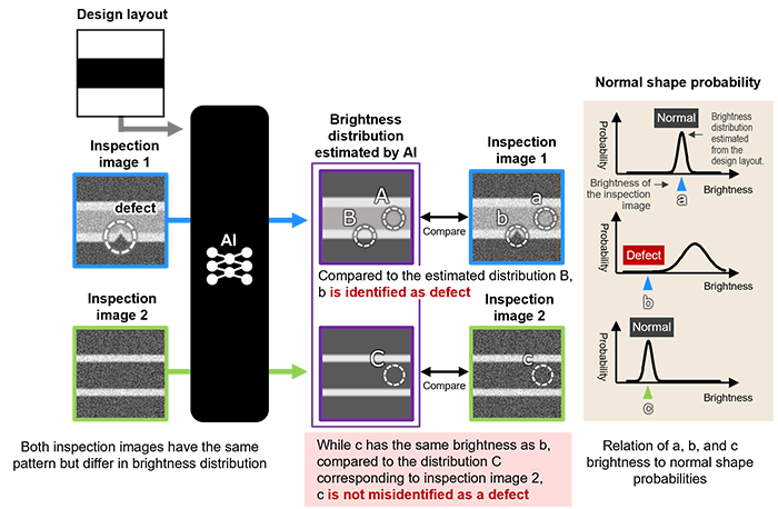
Figure 1. AI technology to estimate the brightness distribution at each observed location on a device
(AI model estimates brightness distributions at each observed location (inspection image 1, inspection image 2) from inspection images and the corresponding design layout. Defect (b) is correctly identified as a defect. While location c has the same brightness as b, the brightness distributions are estimated to be different; accordingly, c is not misidentified as a defect.)
For more information, use the enquiry form below to contact the Research & Development Group, Hitachi, Ltd. Please make sure to include the title of the article.
