Measurement of Cu electrode height with sub-nanometer precision verified using a scanning electron microscope (SEM)
May 10, 2024
Hitachi has developed image processing technology with Hitachi Hight-Tech for measuring minute height differences between Cu electrode patterns that affect the electrical connection state after the semiconductor wafer bonding process.
As stacking (3D IC packaging) technology has come into use, attention is being focused on a new process called hybrid bonding. In this process, Cu (copper) electrode patterns formed on a wafer surface are directly bonded, thereby realizing fast and high-density electrical connections between wafers. Since the connection state depends on the height difference between Cu electrodes before bonding, there has been a need for technology to measure this difference simply and with high precision.
We have therefore developed a Cu electrode height difference measurement method, making use of a scanning electron microscope with backscattered electron detectors positioned at four azimuth angles. Based on the observation that backscattered electron signals emitted from shallow angles are dependent on angle of inclination θ of the sample surface, signal differences between opposing detectors were used to calculate height index. Performance and efficacy were verified jointly with the Belgian international research institution imec.*1 In experimentation comparing this technology with atomic force microscopy (AFM), the developed index is correlated with changes in Cu electrode height, showing the prospect of being able to measure height differences with sub-nanometer precision. (Figure 1)
Hitachi and Hitachi Hight-Tech will continue to work toward practical implementation of this technology as the wafer-to-wafer bonding process comes into common use, contributing to improved semiconductor productivity.
Hitachi announced this technology at the SPIE Advanced Lithography + Patterning 2024 conference that took place February 25 to 29, 2024.
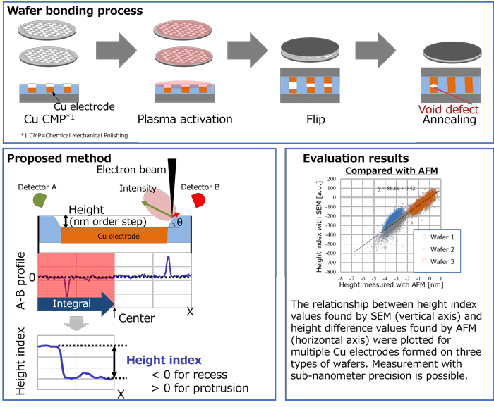
Figure 1. Technology using SEM to evaluate Cu electrode height differences in the semiconductor wafer bonding process
(Height index was proposed based on the observation that the signal difference between opposing detectors A and B in the SEM is dependent on angle of inclination θ.
Cu electrode height index measurements were correlated with height index measurements by AFM with sub-nanometer precision.)
For more information, use the enquiry form below to contact the Research & Development Group, Hitachi, Ltd. Please make sure to include the title of the article.
