GLOBAL INNOVATION REPORT
Latest Technology Trends and VLC Photonics S.L. (Spain) Initiatives
Integrated circuits have revolutionized the world by being built into many devices since the 1960’s. A similar revolution is coming with the possibility of low-cost, high-volume integration and miniaturization of optical components into PICs. This article describes PIC technology, its contribution to society, and Hitachi High-Tech's development services.


Figure 1 | Example PIC with Different Integrated Optical Elements (Center), Optical Waveguides (Left), and Dimensions of a Typical Chip (Right)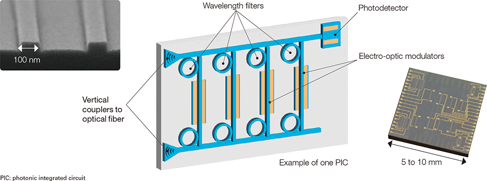
Figure 2 | PIC Applications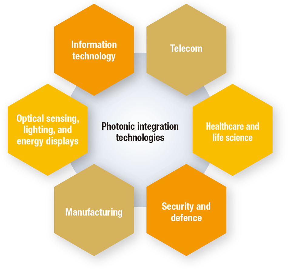
Electronic integrated circuits have revolutionized the world by embedding miniature components in hundreds of millions of devices at different markets since the 1960’s, when basic components like transistors, resistors or capacitors could be integrated into a monolithic silicon wafer die. These tiny chips could be mass produced by the millions using lithography at a very low cost, enabling to embed multiple functionalities and complex architectures into very robust and reliable microelectronic components.
In a similar fashion, but a few decades later, a similar revolution is coming with the possibility of miniaturizing optical components into photonic integrated circuits (PICs) at low cost and high volumes. Photonic components like light emitters (lasers), light detectors (photodiodes) and others (modulators, filters, etc.) can now be integrated as well into monolithic PICs (see Figure 1). Such possibility enables all the advantages of integration for applications where such optical components are used, for example fiber optic communications (both long-distance telecom networks and short distance datacenter links), laser-based radar [light detection and ranging (LiDAR)] mainly for autonomous vehicles, quantum computing and cryptography, and light-based medical instruments, healthcare wearables and diagnostic lab-on-a-chip devices (see Figure 2).
These PICs use silicon as substrate material as well, although they can use other material platforms*1, each having its own advantages and disadvantages. All the technology and processes developed over the years for the micro-electronics industry can now be reused for PICs, saving costs and accelerating time-to-market. This is making that the adoption for them is growing at an amazing pace in some markets, and investment on the technology is flourishing globally.
Many semiconductor business models are being adopted in photonics as well, like the pure-play foundries that fabricate for fabless companies, so foundries amortize faster on their investment by loading their lines as much as they can with many customers, while these don’t need to invest huge amounts in setting up a fab in a clean-room. Other models are that of design houses, providing outsourced component design and circuit layout, or the outsourced assembly and test companies that take care of the very challenging back-end, much more complex than in electronics due to the 100x size reduction between electrical and optical input/output ports.
There are many good reasons why PICs are being adopted by many industries:
The next sections describe more in detail some of the example applications that have been presented above.
Silicon PICs and other variants like SiN or III-V materials (mostly InP), have been attracting considerable interest as they encourage the fabrication of very complex photonic chips for high-performance optical communications. PICs have the potential for enabling high density, high data rates and flexible solutions not only in optical telecommunication networks, but also in datacenter communications. From intra-chip to chip-to-chip and chip-to-board, PIC technology can provide significant advantages.
It is expected that PICs must achieve not only increased performance, but effective reliability and economic scalability to become competitive in those markets. PICs, as opposed to discrete optical components like individual lasers or photodiodes, combine more than one optical function on a single chip. The functions can be active functions such as optical signal generation, optical modulation, or photodetection, as well as passive functions such as optical signal routing or filtering. PICs provide a means for significantly reducing system size, weight, and power, improving reliability, and increasing system performance and functionality. Traditionally, optical communication systems like transceivers are built from discrete components and the components are connected together using fiber connections. This is cumbersome in that each time light is coupled from a device to an optical fiber, or from an optical fiber to a device, signal power is reduced. PICs can overcome these issues by connecting components on the chip using optical waveguides. They can realize novel system architectures employing advanced modulation formats where systems built from discrete components might be too complex and negatively impact size, weight, and power requirements.
However, like any other emerging technologies, PIC design comes with several specific challenges such as thermal management, photonic packaging, radio frequency interface management for high-speed control electronics, and overall circuit modelling, which demand concerted efforts to be addressed. Today, there is a strong movement towards co-packaging and on-board optics. These technologies need to be able to support faster photonic devices such as >80 GHz silicon modulators that can operate at very high speeds*2. There are other modulator technologies that are being developed with both high speed and low power potential that include: polymer, slot, plasmonic, thin-film lithium niobate, or barium titanate among others.
Overall, data centers need faster optical devices, higher integration levels, higher reliability, lower power consumption, a higher degree of scalable economics that address $/Gbps metrics, and smaller more miniaturized foot-print platforms. Co-packaged solutions with hybrid integration between different technologies are required. The integration of electronics, photonics, and packaging is an important need that the industry is addressing today and will explore this in more intensity over the next decade.
LiDAR, short for light detection and ranging or “light radar,” is used to measure distances with high resolution and precision by illuminating the object with a scanning laser beam, and consequently measuring the reflections. A LiDAR basically consists of a laser source, a laser beam scanner, and the detection optics. Various techniques are used to combine these elements into a functional system, such as pulsed, flash and frequency-modulated LiDAR. As an example, many companies are working on bringing a PIC-based frequency modulated continuous-wave (FMCW) LiDAR to the market, that can detect not only the distance, but also the speed of target objects.
The opportunities for using LiDAR are plenty, most notably in automotive, where it is used in advanced driver-assistance systems (ADAS) and in autonomous driving, providing a better resolution than radar. Over the last decade, pushed by the automotive market, the price of LiDAR systems has come down by more than an order of magnitude.
PICs offer new opportunities for cost-efficient LiDAR, as they can allow for on-chip high density integration of the optical components required and can be massively manufactured in volumes. PICs can be used as the LiDAR laser source: when combined with the on-chip components typically used in communications technology, pulsed lasers and frequency-modulated lasers can be realized. An added advantage is that PICs are typically designed for operation around the telecom wavelengths of 1,310 and 1,550 nm, which is a sweet spot for LiDAR due to eye-safety requirements. This allows the range to be extended significantly, to over 200 m.
PICs can also be used to replace the beam-steering part of the LiDAR, with optical phased arrays. Such optical phased arrays can shape the laser beam and steer it fast for video-rate three-dimensional imaging. Laboratory based implementations have already shown the feasibility, and the technology is now moving to the market. Sources and detectors can be integrated on the beam-steering PIC as well, with the potential of realizing a fully integrated, single-chip LiDAR, and allowing unprecedented high volumes at low cost. Moreover, this technology allows for close integration with electronics.
As an example, a chip-scale FMCW LiDAR system that incorporates wavelength tuning and phased array operation enables two-dimensional non-mechanical beam steering(1).
Recent developments in chip-based photonic quantum circuits have radically impacted quantum information processing. One of the most promising applications is quantum computing(2). Quantum computers will solve complex problems that today’s most powerful supercomputers cannot solve. Rather than store information using bits, quantum computers use quantum bits, or qubits, to encode information as 0s, 1s, or both at the same time. This superposition of states enables quantum computers to manipulate enormous combinations of states at once.
Quantum computers are exceedingly difficult to engineer, build and program. As a result, they are crippled by errors in the form of noise, faults, and loss of quantum coherence, which is crucial to their operation. This loss of coherence (called decoherence), caused by vibrations, temperature fluctuations, electromagnetic waves, ultimately destroys the quantum properties of the computer.
PICs can overcome many of these limitations by implementing the core functionalities of future quantum computers. A sampling algorithm, a procedure that takes a random sample of data, at a speed beyond the reach of classical computers, has been implemented in a PIC on a silicon nitride chip that is compatible with the fabrication processes used by the semiconductor industry(3).
In the wake of the fourth industrial revolution, when data is collected, transferred, and stored in networks at a global scale, cybersecurity and cryptography are of utmost importance. Technologies such as the Internet of Things (IoT), AI or the blockchain increase the data traffic across the networks from their generation locations to cloud-based data repositories. The daily operation of businesses, administrations, and individuals are increasingly confronted with the transmission of sensitive—if not critical—data that require protection, notably against threats to its long-term confidentiality.
Modern cryptography provides fundamental tools to enable digital security in our society. Invented 40 years ago, public-key cryptography enables secure communication over open networks, i.e., the Internet. Computational cryptography however faces challenges: widely deployed public-key techniques are vulnerable to the advent of a quantum computer. Cryptographic protocols relying on classical techniques are vulnerable to undetected eavesdropping and to “store now-attack later*3” attacks. By combining physical layer technologies and quantum information, quantum cryptography offers unique tools to address these challenges.
The most prominent quantum cryptographic protocol is quantum key distribution (QKD)(4), which allows two remote network nodes to generate an encryption key with information theoretic security (ITS). Tremendous technological progress has been achieved in the last two decades in QKD research, culminating in the deployment of QKD over optical fiber communication networks. QKD systems need to evolve technologically towards co-existence with standard coherent optical communication systems and towards miniaturization to achieve cost-effectiveness and scalability. PIC components such as quantum random number generators(5), QKD emitters and receivers will thus make a leap towards QKD on a chip, which would lead to 100 times reduction in price and 10 to 50 times reduction in system volume.
VLC Photonics S.L. (HVLC), a Hitachi High-tech Group company since November 2020, was established by researchers involved for over 20 years in PIC technologies and photonic communication systems, and spin off from the Telecommunications and Multimedia Applications Institute (iTEAM) at Universitat Politècnica de València (UPV), Spain. HVLC is a resident company in the UPV fab cleanroom, the microfabrication research and development and pilot line at UPV (see Figure 3). At first the company started its business as a PIC design company and it continued evolving to respond to the growing needs of PIC adoption. Now the company offers development services for customers in many application markets, including the ones mentioned above on photonic communications (mainly fiber optics), autonomous driving, sensing, signal processing, biomedical, and quantum. HVLC offers nowadays the following PIC development services: consultancy, design, fabrication, characterization/test, and packaging/assembly (see Figure 4)(6). The company also collaborates with Fortune 500 companies and startups, and some world-famous researchers.
Welcoming HVLC to the family, Hitachi High Tech Group will further enhance its engineering services and will contribute to customers with its solutions.
Figure 3 | Cleanroom Personnel Supporting VLC Photonics PIC Testing Services (Left) and Technician Adjusting the Automated PIC Testing Tool (Right)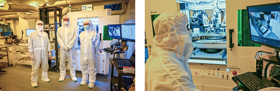
Figure 4 | Cycle of the Service Provided by VLC Photonics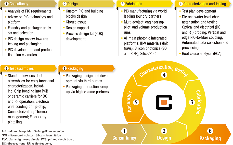
Photonic integration technology is positioned to be a key enabling technology for many high-tech applications over the next years: from optical communication transceivers to LiDAR or gyroscope sensors for autonomous cars, cryptographic applications for banking and secure commerce and communications, or medical instrumentation and healthcare wearable devices. While there are many challenges to mature and scale the technology to the level that electronic integration has reached over the last decades, the potential for growth is phenomenal, and there will be many other applications that benefit from this technology in the future too.
