New technology will contribute to realizing a decarbonized society by enabling product design aligned with a wide range of customer applications
September 9, 2021
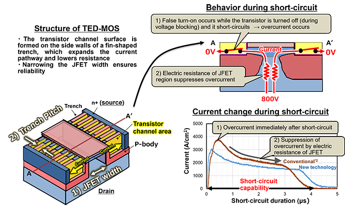
Figure 1: Structure of TED-MOS and physical model for short-circuit characteristics
With the aim of helping achieve a decarbonized society, Hitachi previously developed TED-MOS*1, a power device with an innovative structure that uses the next-generation material silicon carbide (SiC) and delivers improved ruggedness and low power consumption characteristics*2, *3. It has now established a physical model relating to the suppression mechanism for overcurrent, which causes breakdowns when a device short-circuits*4. Furthermore, based on this physical model, it has developed highly flexible device design technology that leverages the structural advantages of TED-MOS. This has made it possible to eliminate the trade-off between ruggedness and low power consumption characteristics that is an issue with conventional power devices that incorporate silicon-based materials, thereby supporting increased energy-efficiency and energy-saving performance for power electric devices used for a wide range of purposes by customers. Going forward, Hitachi aims to further improve the performance of TED-MOS and develop a wide range of applications for the product, such as energy systems, electrical vehicles, and data centers.
Some of these findings were published at the 33rd International Symposium on Power Semiconductor Devices and ICs (ISPSD) held from May 31 to June 3, 2021.
Because SiC power devices have higher dielectric breakdown electric field strength compared with conventional devices that use silicon (Si), it is possible to reduce the thickness of the devices, making them suitable for low-resistance, high-frequency switching. However, the following is an issue: because the dielectric breakdown electric field strength is high when the device is turned off, it is difficult to ensure the product’s lifetime if a short-circuit occurs due to a malfunction.
In order to resolve this issue, Hitachi has established a physical model for suppressing overcurrent by focusing on the behavior of the current during a short-circuit, as shown in Figure 1—especially the phenomenon of overcurrent due to the short-circuit attenuating after it peaks. Here, the length of time after overcurrent occurs during which the device is able to withstand it without a breakdown is defined as the “short-circuit capability,” which is used as an indicator representing ruggedness. The process via which a device short-circuits may be viewed as follows: 1) overcurrent flows due to the transistor status falsely becoming on while the device is turned off (while the voltage is being blocked); 2) the current density of the JFET*5 in the device’s center increases and the temperature rises locally; and 3) the JFET resistance grows due to the rise in temperature and the overcurrent attenuates. To improve the short-circuit capability, it is necessary to suppress overcurrent, which causes device breakdown. Typically, the greater the electrical resistance of the transistor region, the lower the overcurrent will be during a short-circuit, so the electrical resistance of the transistor region and short-circuit capability may be considered to have a trade-off relationship. However, if, based on the physical model of item 3 above which is the focus here, it was possible to develop a structure with which there was a significant increase in resistance due to JFET heat generation when a device short-circuits, it would be possible to reduce overcurrent during the short-circuit and there would be no growth in the electrical resistance of the transistor region, enabling improvement of the short-circuit capability.
With TED-MOS, as shown in Figure 1, the vertical and horizontal design parameters for the trench (groove) pitch are independent of each other. As a result, it is possible to design the electrical resistance of the transistor region and the electrical resistance of the JFET region independently. Hitachi has leveraged this advantage to develop device design technology that reflects the knowledge obtained based on the above physical model. Specifically, by setting the JFET width as the parameter for suppressing heat generation when the device short-circuits and setting the trench pitch as the parameter for controlling the electrical resistance of the transistor region, it tried to design the short-circuit capability and on resistance*6 (an indicator of power consumption) independently. When the trench pitch, which is a design parameter specific to TED-MOS, is narrowed, the trench’s surface area and the the channel*7 area through which current flows increase, decreasing the electrical resistance in the transistor region.
As shown in Figure 2, in device evaluation results for various designs that were actually produced, the on resistance (power consumption indicator) was used as the vertical axis and the short-circuit capability (ruggedness indicator) as the horizontal axis. In Figure 2, the trade-off of conventional devices*2 is shown by the dotted line and black dots: as the JFET width increases, the on resistance decreases and the short-circuit capability deteriorates. The new data obtained with this technology is shown by the areas in orange and blue. The JFET width is 1.0 μm and 0.9 μm, respectively. Simply by reducing the JFET width from 1.0 μm to 0.9 μm, the on resistance grows even though the short-circuit capability improves (trend shown by arrow 1). However, if the trench pitch is narrowed and the electrical resistance in the transistor region is decreased without changing the JFET width, it was confirmed that the short-circuit capability is maintained and only the on resistance is reduced (trend shown by arrow 2). Likewise, for the sample group with a JFET width of 1.0 μm shown in orange, the short-circuit capability was maintained and only the on resistance was reduced. Thus, the evaluation confirmed that with the TED-MOS device structure, it is possible to design the short-circuit capability and on resistance independently by adjusting the JFET width and trench pitch as design parameters.
Going forward, using this technology, Hitachi will eliminate the trade-off between ruggedness and low power consumption performance that was previously an issue and supply power devices with high design flexibility suited to a wide range of customer uses, thereby contributing to the realization of a decarbonized society by reducing power consumption for products used in social infrastructure and decreasing carbon dioxide emissions.
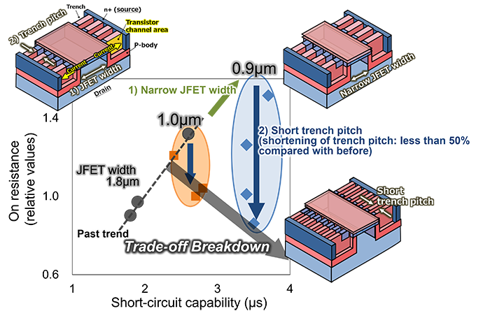
Figure 2: Elimination of trade-off between on resistance and short-circuit capability based on highly flexible device design technology
For more information, use the enquiry form below to contact the Research & Development Group, Hitachi, Ltd. Please make sure to include the title of the article.
